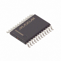
DS1780E/T&R Maxim Integrated Products, DS1780E/T&R Datasheet - Page 9

DS1780E/T&R
Manufacturer Part Number
DS1780E/T&R
Description
IC CPU PERIPHERAL MON 24-TSSOP
Manufacturer
Maxim Integrated Products
Datasheet
1.DS1780E.pdf
(28 pages)
Specifications of DS1780E/T&R
Function
Thermal Monitor, CPU Peripherals
Topology
ADC (Sigma Delta), Comparator, Fan Speed Control, Register Bank
Sensor Type
Internal
Sensing Temperature
-40°C ~ 125°C
Output Type
I²C™/SMBus™
Output Alarm
No
Output Fan
Yes
Voltage - Supply
2.8 V ~ 5.75 V
Operating Temperature
-40°C ~ 125°C
Mounting Type
Surface Mount
Package / Case
24-TSSOP
Full Temp Accuracy
+/- 12 %
Digital Output - Bus Interface
Serial (2-Wire)
Digital Output - Number Of Bits
8 bit
Maximum Operating Temperature
+ 125 C
Minimum Operating Temperature
- 40 C
Lead Free Status / RoHS Status
Contains lead / RoHS non-compliant
Available stocks
Company
Part Number
Manufacturer
Quantity
Price
Company:
Part Number:
DS1780E/T&RDS1780E/TR
Manufacturer:
XILINX
Quantity:
17
The worse such accident would be connecting -12V to +12V; a total of 24V difference, with the series
resistors this would draw a maximum of approximately 24 ma.
The internal scaling factor depends upon the particular input. The +12V
inputs are internally scaled such that the nominal value of the respective supply corresponds to 3/4 of full
range, or a decimal count of 192. The approximate resolution is thus equal to:
This is depicted below in Table 5.
VOLTAGE/DATA RELATIONSHIPS FOR POSITIVE ONLY VOLTAGE INPUTS
(+12V
The other two voltage inputs use a slightly different scaling technique, due to the nature of the PC voltage
they are monitoring. Because processor voltage (V
inputs are internally scaled such that the ADC result is 0h for a 0V input and the maximum value of FFh
is returned for a voltage of 3.60V. This corresponds to an LSb weighting of 14.1 mV.
The inputs can also be used to monitor a negative supply, such as -12V. However, a resistor ladder and
positive reference voltage (V
swings between OV and +3.6V. Assuming the DS1780 +V
input impedance and the V
LSb (R
ADC RESULT (BASE
LSb WEIGHTING
INPUT PIN
1
IN
, R
(mV)
, +5V
190
191
192
193
252
253
254
255
10)
0
1
2
3
4
•
•
•
•
•
•
2
) @
255
3.6
IN
, +3.3V
é
ê
ë
R
1
PIN VOLTAGE (V)
R
+
1
R
REF
2
IN
ù
ú
û
, and +2.5V
+12V
REF
11.875
11.938
12.063
15.813
15.875
15.938
is a perfect supply, then the resolution and range of -12V input are:
0.063
0.125
0.188
15.75
62.5
0.25
12.0
0
•
•
•
•
•
•
) must be used (see Figure 1) such that input voltage to the DS1780
IN
LSb (V
IN
PIN VOLTAGE (V)
) Table 5
NOM
9 of 28
CCP
+5V
0.026
0.052
0.078
0.104
4.948
4.974
5.026
6.563
6.589
6.615
6.641
) @
26.0
5.0
0
•
•
•
•
•
•
) can vary to 3.6V, the +V
IN
4/3
256
V
NOM
CCP1
PIN VOLTAGE (V)
and +2.5V
+3.3V
0.017
0.034
0.052
0.069
3.266
3.283
3.317
4.331
4.348
4.366
4.383
IN
17.2
3.3
, +5V
0
•
•
•
•
•
•
IN
S
/+V
IN
CCP1
, +3.3V
CCP2
and +2.5V
PIN VOLTAGE (V)
pins have infinite
IN
, and +2.5V
+2.5V
0.013
0.026
0.039
0.052
2.474
2.487
2.513
3.281
3.294
3.307
13.0
3.32
2.5
0
•
•
•
•
•
•
S
/+V
IN
CCP1
IN


