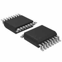
ADM1023ARQZ-REEL ON Semiconductor, ADM1023ARQZ-REEL Datasheet - Page 12

ADM1023ARQZ-REEL
Manufacturer Part Number
ADM1023ARQZ-REEL
Description
IC SENSOR TEMP DUAL PREC 16QSOP
Manufacturer
ON Semiconductor
Datasheet
1.ADM1023ARQZ.pdf
(16 pages)
Specifications of ADM1023ARQZ-REEL
Function
Temp Monitoring System (Sensor)
Topology
ADC, Comparator, Multiplexer, Register Bank
Sensor Type
External & Internal
Sensing Temperature
0°C ~ 120°C, External Sensor
Output Type
SMBus™
Output Alarm
Yes
Output Fan
No
Voltage - Supply
3 V ~ 5.5 V
Operating Temperature
0°C ~ 120°C
Mounting Type
Surface Mount
Package / Case
16-QSOP
Temperature Sensor Function
Temp Sensor
Interface Type
Serial (2-Wire)
Operating Temperature (min)
0C
Operating Temperature (max)
120C
Operating Temperature Classification
Commercial
Operating Supply Voltage (min)
3V
Operating Supply Voltage (typ)
3.3V
Operating Supply Voltage (max)
3.6V
Full Temp Accuracy
+/- 1 C, +/- 3 C
Digital Output - Bus Interface
Serial (2-Wire)
Maximum Operating Temperature
+ 120 C
Minimum Operating Temperature
0 C
Lead Free Status / RoHS Status
Lead free / RoHS Compliant
Available stocks
Company
Part Number
Manufacturer
Quantity
Price
Company:
Part Number:
ADM1023ARQZ-REEL
Manufacturer:
IDT
Quantity:
56
Part Number:
ADM1023ARQZ-REEL
Manufacturer:
ADI/亚德诺
Quantity:
20 000
Table 8. Device Addresses
Figure 15. Writing a Register Address to the Address Pointer Register, then Writing Data to the Selected Register
1. ADD0 and ADD1 are sampled at powerup only.
The serial bus protocol operates as follows:
ADD0
1. The master initiates data transfer by establishing a
NC
NC
NC
0
0
0
1
1
1
start condition, defined as a high−to−low transition
on the serial data line, SDATA, while the serial
clock line, SCLK, remains high. This indicates
that an address/data stream will follow. All slave
peripherals connected to the serial bus respond to
the start condition and shift in the next 8 bits.
These bits consist of a 7−bit address (MSB first)
plus an R/W bit, which determines the direction of
the data transfer, that is, whether data is written to,
or read from, the slave device.
The peripheral whose address corresponds to the
transmitted address responds by pulling the data
line low during the low period before the ninth
SDATA
SCLK
START BY
MASTER
SDATA
SCLK
START BY
MASTER
ADD1
NC
NC
NC
1
0
0
1
0
1
0
1
1
0
1
(Note 1)
SERIAL BUS ADDRESS BYTE
1
0
Figure 16. Writing to the Address Pointer Register Only
SERIAL BUS ADDRESS BYTE
Device Address
0
1
FRAME 1
0101 001
0101 010
1001 100
1001 101
0011 000
0011 001
0011 010
0101 011
1001 110
1
1
FRAME 1
SDATA (CONTINUED)
SCLK (CONTINUED)
A1
1
http://onsemi.com
A0
A1
ADM1023
R/W
A0
ADM1023
ACK. BY
12
R/W
9
ADM1023
ACK. BY
D7
D7
9
1
1
2. Data is sent over the serial bus in sequences of
3. When all data bytes have been read or written,
clock pulse, known as the Acknowledge bit. All
other devices on the bus remain idle while the
selected device waits for data to be read from or
written to it. If the R/W bit is 0, the master writes
to the slave device. If the R/W bit is 1, the master
reads from the slave device.
nine clock pulses, 8 bits of data followed by an
Acknowledge bit from the slave device.
Transitions on the data line must occur during the
low period of the clock signal and remain stable
during the high period, because a low−to−high
transition when the clock is high may be
interpreted as a stop signal. The number of data
bytes that can be transmitted over the serial bus in
a single read or write operation is limited only by
what the master and slave devices can handle.
stop conditions are established. In write mode, the
master pulls the data line high during the 10th
clock pulse to assert a stop condition. In read
mode, the master device overrides the
Acknowledge bit by pulling the data line high
during the low period before the ninth clock pulse.
This is known as No Acknowledge. The master
then takes the data line low during the low period
before the 10th clock pulse, then high during the
10th clock pulse to assert a stop condition.
D7
D6
D6
1
ADDRESS POINTER REGISTER BYTE
D5
D6
D5
ADDRESS POINTER REGISTER BYTE
D4
D5
D4
FRAME 2
DATA BYTE
D4
D3
D3
FRAME 3
FRAME 2
D3
D2
D2
D2
D1
D1
D1
D0
D0
ADM1023
ADM1023
ACK. BY
ACK. BY
D0
9
9
ADM1023
ACK. BY
9
STOP BY
MASTER
STOP BY
MASTER


