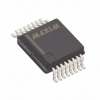
MAX1298CEAE+ Maxim Integrated Products, MAX1298CEAE+ Datasheet - Page 14

MAX1298CEAE+
Manufacturer Part Number
MAX1298CEAE+
Description
IC TEMP SENS W/ADC 16-SSOP
Manufacturer
Maxim Integrated Products
Datasheet
1.MAX1298CEAET.pdf
(20 pages)
Specifications of MAX1298CEAE+
Function
Temp Monitoring System (Sensor)
Topology
ADC, Multiplexer, Register Bank
Sensor Type
External & Internal
Sensing Temperature
-40°C ~ 85°C, External Sensor
Output Type
MICROWIRE™, QSPI™, SPI™
Output Alarm
No
Output Fan
No
Voltage - Supply
4.75 V ~ 5.25 V
Operating Temperature
-40°C ~ 85°C
Mounting Type
Surface Mount
Package / Case
16-SSOP
Full Temp Accuracy
+/- 1 C
Digital Output - Bus Interface
Serial (3-Wire)
Digital Output - Number Of Bits
12 bit
Maximum Operating Temperature
+ 85 C
Minimum Operating Temperature
- 40 C
Lead Free Status / RoHS Status
Lead free / RoHS Compliant
Input data (configuration and conversion bytes) are
clocked into the MAX1298/MAX1299 at DIN on the ris-
ing edge of SCLK when CS is low. The start bit (MSB)
of an input data byte is the first logic 1 bit that arrives:
After CS falls,
after receipt of a complete configuration byte with no
conversion in progress,
after 16 bits have been clocked onto DOUT following a
conversion.
12-Bit Serial-Output Temperature Sensors
with 5-Channel ADC
Figure 4. Detailed Serial Interface Timing
Figure 5. Bipolar Transfer Function
14
011111111111
011111111110
000000000010
000000000001
000000000000
111111111111
111111111110
111111111101
100000000010
100000000001
______________________________________________________________________________________
OUTPUT CODE
- FS + 1LSB
DOUT
SCLK
+ FS = + 2V
- FS = - 2V
1LSB = 2V
DIN
CS
2048
REF
REF
REF
t
OR
OR
CSO
X
IN + - IN - (LSB)
t
DS
0
t
t
DV
CSS
VALID
Input Data Format
t
+ FS - 1LSB
CH
t
DH
X
t
CL
t
DO
VALID
Output data from the MAX1298/MAX1299 are clocked
onto DOUT on the falling edge of SCLK in the form of two
8-bit words, MSB first (Table 1). For temperature conver-
sions, the output is 12-bit binary (D10–S0) padded with 2
leading extraneous bits and two trailing zeros. For volt-
age conversions, the output is 12-bit two’s-complement
binary (D11–D0) with 1 sub-bit and two trailing zeros.
Figure 5 shows the bipolar transfer function.
On power-up, the MAX1298/MAX1299 defaults to shut-
down mode. Start a conversion by transferring a configu-
ration byte and a conversion byte into DIN with the
control formats shown in Tables 2 and 3, respectively.
(See Power Modes for related discussion.)
SSTRB goes low on the falling edge of the last bit of the
conversion byte, and it returns high when the conversion
is complete. For best noise performance, SCLK should
remain low while SSTRB is low. Typical conversion times
are 2.2ms for temperature measurements and 1.1ms for
voltage measurements. The MSB of the 2 output bytes is
present at DOUT starting at the rising edge of SSTRB.
Successive SCLK falling edges shift the two 8-bit data
bytes out from an internal register. Additional (>16)
SCLK edges will result in zeros on DOUT.
SSTRB does not go into a high-impedance state when
CS goes high. Pulling CS high prevents data from
being clocked in or out, but it does not adversely affect
a conversion in progress. Figure 6 shows SSTRB timing
details.
Subsequent conversions with the same reference mode
do not require a configuration byte.
VALID
t
CSH
X
Performing a Conversion
t
CS
t
CS1
t
TR
Output Data Format


