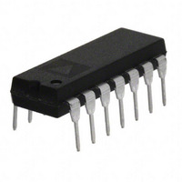
AD650KN Analog Devices Inc, AD650KN Datasheet - Page 9

AD650KN
Manufacturer Part Number
AD650KN
Description
IC V-F/F-V CONVERTER 14-DIP
Manufacturer
Analog Devices Inc
Type
Volt to Freq & Freq to Voltr
Datasheet
1.AD650KNZ.pdf
(20 pages)
Specifications of AD650KN
Mounting Type
Through Hole
Rohs Status
RoHS non-compliant
Frequency - Max
1MHz
Full Scale
±150ppm/°C
Linearity
±0.1%
Package / Case
14-DIP (0.300", 7.62mm)
Full Scale Range
1MHz
Linearity %
0.005%
Supply Voltage Range
± 9V To ± 18V
Digital Ic Case Style
DIP
No. Of Pins
14
Peak Reflow Compatible (260 C)
No
Converter Function
VFC/FVC
Full Scale Frequency
1000
Power Supply Requirement
Dual
Single Supply Voltage (typ)
Not RequiredV
Single Supply Voltage (max)
Not RequiredV
Single Supply Voltage (min)
Not RequiredV
Dual Supply Voltage (min)
±9V
Dual Supply Voltage (max)
±18V
Operating Temperature (min)
0C
Operating Temperature (max)
70C
Operating Temperature Classification
Commercial
Package Type
PDIP
Calibration Error Fs Typ
5%
Rohs Compliant
No
Lead Free Status / Rohs Status
Not Compliant
Available stocks
Company
Part Number
Manufacturer
Quantity
Price
Part Number:
AD650KN
Manufacturer:
ADI/亚德诺
Quantity:
20 000
Company:
Part Number:
AD650KNZ
Manufacturer:
Analog Devices Inc
Quantity:
135
Company:
Part Number:
AD650KNZ
Manufacturer:
AD
Quantity:
3 012
If the approximate amount of noise that appears on C
(V
inequality:
For example, consider an application calling for a maximum
frequency of 75 kHz, a 0 V to 1 V signal range, and supply
voltages of only ±9 V. The component selection guide of Figure 9
is used to select 2.0 kΩ for R
in a one-shot time period of approximately 7 μs. Substituting
75 kHz into Equation 7 yields a value of 1300 pF for C
the input signal is near zero, 1 mA flows through the integration
capacitor to the switched current sink during the reset phase,
causing the voltage across C
Because the integrator output stage requires approximately 3 V
headroom for proper operation, only 0.5 V margin remains for
integrating extraneous noise on the signal line. A negative noise
pulse at this time could saturate the integrator, causing an error
in signal integration. Increasing C
provides much more noise margin, thereby eliminating this
potential trouble spot.
NOISE
C
), then the value of C
INT
>
+
t
V
OS
S
−
×
3
1
V
×
10
−
V
−
3
NOISE
INT
INT
A
IN
can be checked using the following
to increase by approximately 5.5 V.
and 1000 pF for C
INT
to 1500 pF or 2000 pF
OS
. This results
INT
INT
is known
. When
Rev. D | Page 9 of 20
(8)
100kHz
10kHz
1MHz
1000
100
20
INPUT
RESISTOR
Figure 10. Typical Nonlinearity vs. C
Figure 9. Full-Scale Frequency vs. C
16.9k
40.2k
100k
50
20k
50
100
ONE SHOT CAPACITOR
100
C
OS
C
(pF)
OS
(pF)
1000
1000
OS
OS
INPUT
RESISTOR
16.9k
20k
40.2k
100k
AD650


