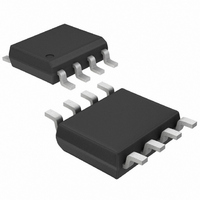
MAX6145ESA+T Maxim Integrated Products, MAX6145ESA+T Datasheet - Page 7

MAX6145ESA+T
Manufacturer Part Number
MAX6145ESA+T
Description
IC REF VOLT 4.5V 8-SOIC
Manufacturer
Maxim Integrated Products
Datasheet
1.MAX6141EURT.pdf
(9 pages)
Specifications of MAX6145ESA+T
Reference Type
Series
Voltage - Output
4.5V
Tolerance
±1%
Temperature Coefficient
50ppm/°C
Voltage - Input
4.7 ~ 12.6 V
Number Of Channels
1
Current - Quiescent
105µA
Current - Output
1mA
Operating Temperature
-40°C ~ 85°C
Mounting Type
Surface Mount
Package / Case
8-SOIC (3.9mm Width)
Product
Voltage References
Topology
Series References
Output Voltage
4.5 V
Initial Accuracy
1 %
Average Temperature Coefficient (typ)
50 PPM / C
Series Vref - Input Voltage (max)
13.5 V
Maximum Operating Temperature
+ 85 C
Minimum Operating Temperature
- 40 C
Mounting Style
SMD/SMT
Lead Free Status / RoHS Status
Lead free / RoHS Compliant
Current - Cathode
-
Lead Free Status / Rohs Status
Lead free / RoHS Compliant
Set the output voltage on the MAX6160 by connecting
a resistor divider between OUT, ADJ, and GND
(Figure 1). Choose R1 according to the following equa-
tion:
where V
compensates for the MAX6160's change in ADJ input
current over temperature. When R1 is chosen correctly,
the change in voltage across R1 caused by the ADJ
input current is properly cancelled. Choose R1 to within
*Except MAX6160.
**MAX6160 only.
Figure 1. MAX6160 Adjustable Output Circuit
_____________Applications Information
______________________________________________________________Pin Description
2, 3, 5*, 6, 7
Setting the MAX6160 Output Voltage
SO
TH
5**
1
4
8
R1 = (1.06 x 10
MAX6160
= 1.23V. The scaling factor (1.06 x 10
GND
V
IN
IN
OUT
_______________________________________________________________________________________
ADJ
PIN
SOT23-3
5
—
—
2
3
1
) (V
R1
R2
OUT
V
OUT
/ V
R1 = 1.06 x 10
R2 = –—––––
V
ADJ
SOT143
(
ADJ
–––– - 1
= 1.23V
V
V
OUT
ADJ
SOT23, Low-Cost, Low-Dropout,
—
4
1
2
3
R1
) Ω
3-Terminal Voltage References
5
)
(
––––
V
V
OUT
ADJ
)
Ω
NAME
GND
OUT
N.C.
ADJ
IN
5
)
Reference Output
No Connection. Not internally connected.
Ground
Adjustable output voltage feedback input. Connect a resistor
divider between OUT, ADJ, and GND (Figure 1).
Input Voltage
±5% of this calculated value (nearest standard value
plus specified resistor tolerance) to optimize the output
voltage temperature coefficient. Using R1 = 215kΩ:
which is also the nearest 0.1% resistor value.
Choose R2 according to the following equation:
For example, a 2.5V output requires R1 = (1.06 x 10
(2.5V / 1.23V) ≈ 215kΩ, which is the nearest standard-
value 0.1% resistor.
For the best line-transient performance, decouple the
input with a 0.1µF ceramic capacitor, as shown in the
Typical Operating Circuit. Locate the capacitor as
close to the device pin as possible. Where transient
performance is less important, no capacitor is
necessary.
The MAX6125/MAX6141/MAX6145/MAX6150/MAX6160
do not require an output capacitor. They are stable for
capacitive loads from 0nF to 10nF. If your application
requires an output charge reservoir (e.g., to decouple
the reference from a DAC’s input), then make sure that
the total output capacitive load does not exceed 10nF
for optimum settling-time performance.
R2 = R1 / (V
R2 =
FUNCTION
1.23V
OUT
2.5V
215k
/ V
Ω
- 1
ADJ
Output Bypassing
- 1)
≈
Input Bypassing
208k
Ω
5
7
)


