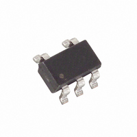
MAX6129AEUK30+T Maxim Integrated Products, MAX6129AEUK30+T Datasheet - Page 7

MAX6129AEUK30+T
Manufacturer Part Number
MAX6129AEUK30+T
Description
IC REF VOLT 3.00V SOT23-5
Manufacturer
Maxim Integrated Products
Datasheet
1.MAX6129BEUK25T.pdf
(16 pages)
Specifications of MAX6129AEUK30+T
Reference Type
Series
Voltage - Output
3V
Tolerance
±0.4%
Temperature Coefficient
40ppm/°C
Voltage - Input
3.2 ~ 12.6 V
Number Of Channels
1
Current - Quiescent
6.75µA
Current - Output
4mA
Operating Temperature
-40°C ~ 85°C
Mounting Type
Surface Mount
Package / Case
SOT-23-5, SC-74A, SOT-25
Product
Voltage References
Topology
Series References
Output Voltage
3 V
Initial Accuracy
0.4 %
Average Temperature Coefficient (typ)
40 PPM / C
Series Vref - Input Voltage (max)
13 V
Shunt Current (max)
4 mA
Maximum Operating Temperature
+ 85 C
Minimum Operating Temperature
- 40 C
Mounting Style
SMD/SMT
Lead Free Status / RoHS Status
Lead free / RoHS Compliant
Current - Cathode
-
Lead Free Status / Rohs Status
Lead free / RoHS Compliant
ELECTRICAL CHARACTERISTICS—MAX6129_50 (V
(V
Note 1: MAX6129 is 100% production tested at T
Note 2: Temperature coefficient is defined by box method: (V
Note 3: Not production tested. Guaranteed by design for both SOT23 and dice.
Note 4: Only the typical values apply to MAX6129A sold in die form (max values apply to packaged parts).
Note 5: Thermal hysteresis is defined as the change in output voltage at T
Note 6: Dropout voltage is the minimum input voltage at which V
OUTPUT
Output Voltage
Output Voltage Temperature
Coefficient (Notes 2, 3)
Line Regulation (Note 4)
Load Regulation (Note 4)
Dropout Voltage (Notes 4, 6)
Output Short-Circuit Current
Long-Term Stability
Thermal Hysteresis
DYNAMIC CHARACTERISTICS
Noise Voltage
Ripple Rejection
Turn-On Settling Time
INPUT
Supply Voltage Range
Supply Current
Change in Supply Current
(Note 4)
IN
= 5.2V, I
to T
Load Regulation Test.
PARAMETER
MIN
OUT
Ultra-Low-Power Series Voltage Reference
.
= 0, T
_______________________________________________________________________________________
A
= T
MIN
to T
MAX
∆V
∆V
∆V
V
SYMBOL
TCV
IN
∆V
OUT
OUT
I
∆I
OUT
V
e
IN
, unless otherwise noted. Typical values are at T
V
I
- V
OUT
OUT
I
OUT
OUT
SC
t
IN
/V
R
IN
OUT
/∆V
/∆V
/time 1000 hours at +25°C
OUT
IN
/
IN
IN
A
T
MAX6129A
MAX6129B
V
I
I
I
I
(Note 5)
f = 0.1Hz to 10Hz
f = 10Hz to 1kHz
V
To V
V
OUT
OUT
OUT
OUT
= +25°C and is guaranteed by design for T
A
IN
IN
IN
= +25°C
= 5.2V to 12.6V
= 5.2V ±200mV, f = 120Hz
= 5.2V to 12.6V
OUT
= 0 to 4mA
= 0 to -1mA
= 0
= 4mA
= 0.1% of final value
MAX
CONDITIONS
OUT
- V
MIN
changes by 0.1% from V
)/(∆T
MAX6129A (±0.4%)
MAX6129B (±1%)
A
= +25°C before and after cycling the device from T
OUT
✕
V
+25°C
= 5.000V)
).
A
= +25°C.) (Note 1)
OUT
A
4.9800
4.9500
= T
MIN
5.2
at rated V
MIN
to T
5.0000
5.0000
0.175
TYP
140
150
140
245
0.3
3.3
1.4
1.0
34
25
90
38
MAX
IN
and is guaranteed by
as specified.
5.0200
5.0500
MAX
12.6
10.5
100
375
100
200
0.8
1.5
40
9
ppm/°C
UNITS
µV
µV/µA
µV
µV/V
ppm
ppm
µA/V
mV
mA
ms
dB
µA
V
RMS
V
P-P
MAX
7


