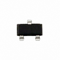
LM4051AEM3-ADJ/NOPB National Semiconductor, LM4051AEM3-ADJ/NOPB Datasheet - Page 5

LM4051AEM3-ADJ/NOPB
Manufacturer Part Number
LM4051AEM3-ADJ/NOPB
Description
IC REF PREC MICROPWR ADJ SOT23-3
Manufacturer
National Semiconductor
Datasheet
1.LM4051CIM3-1.2NOPB.pdf
(14 pages)
Specifications of LM4051AEM3-ADJ/NOPB
Reference Type
Shunt, Adjustable
Voltage - Output
1.24 ~ 10 V
Tolerance
±0.1%
Temperature Coefficient
50ppm/°C
Number Of Channels
1
Current - Cathode
60µA
Current - Output
12mA
Operating Temperature
-40°C ~ 125°C
Mounting Type
Surface Mount
Package / Case
SOT-23-3, TO-236-3, Micro3™, SSD3, SST3
Lead Free Status / RoHS Status
Lead free / RoHS Compliant
Voltage - Input
-
Current - Quiescent
-
Other names
LM4051AEM3-ADJ
LM4051AEM3-ADJTR
LM4051AEM3-ADJTR
LM4051-ADJ (Adjustable)
Electrical Characteristics
Note 1: Absolute Maximum Ratings indicate limits beyond which damage to the device may occur. Operating Ratings indicate conditions for which the device is
functional, but do not guarantee specific performance limits. For guaranteed specifications and test conditions, see the Electrical Characteristics. The guaranteed
specifications apply only for the test conditions listed. Some performance characteristics may degrade when the device is not operated under the listed test
conditions.
Note 2: The maximum power dissipation must be derated at elevated temperatures and is dictated by T
ambient thermal resistance), and T
number given in the Absolute Maximum Ratings, whichever is lower. For the LM4051, T
is 280˚C/W for the SOT-23 package.
Note 3: The human body model is a 100 pF capacitor discharged through a 1.5 kΩ resistor into each pin. The machine model is a 200 pF capacitor discharged
directly into each pin.
Note 4: Typicals are at T
Note 5: Limits are 100% production tested at 25˚C. Limits over temperature are guaranteed through correlation using Statistical Quality Control (SQC) methods.
The limits are used to calculate National’s AOQL.
Note 6: The boldface (over-temperature) limit for Reverse Breakdown Voltage Tolerance is defined as the room temperature Reverse Breakdown Voltage Tolerance
T
max∆T=65˚C is shown below:
Therefore, as an example, the A-grade LM4051-1.2 has an over-temperature Reverse Breakdown Voltage tolerance of
Note 7: When V
the die (-) output and the package (-) output pin. See the Output Saturation curve in the Typical Performance Characteristics section.
Note 8: Reference voltage and temperature coefficient will change with output voltage. See Typical Performance Characteristics curves.
Note 9: Long term stability is V
Note 10: Thermal hysteresis is defined as the difference in voltage measured at +25˚C after cycling to temperature -40˚C and the 25˚C measurement after cycling
to temperature +125˚C.
±
[(∆V
MAX
A-grade:
B-grade:
C-grade:
R
or T
/∆T)(max ∆T)(V
MIN
±
±
±
, and V
0.425% =
0.525% =
0.825% =
OUT
≤ 1.6V, the LM4051-ADJ in the SOT-23 package must operate at reduced I
R
R
is the reverse breakdown voltage. The total over-temperature tolerance for the different grades in the industrial temperature range where
)]. Where, ∆V
J
±
±
±
= 25˚C and represent most likely parametric norm.
0.1%
0.2%
0.5%
R
±
±
±
@
50 ppm/˚C x 65˚C
50 ppm/˚C x 65˚C
50 ppm/˚C x 65˚C
A
25˚C measured during 1000 hrs.
(ambient temperature). The maximum allowable power dissipation at any temperature is PD
R
/∆T is the V
R
temperature coefficient, max∆T is the maximum difference in temperature from the reference point of 25 ˚C to
(Continued)
5
Jmax
= 125˚C, and the typical thermal resistance (θ
R
. This is caused by the series resistance of the die attach between
Jmax
(maximum junction temperature), θ
±
1.2V x 0.425% =
max
JA
= (T
), when board mounted,
±
Jmax
5.2 mV.
− T
www.national.com
JA
A
)/θ
(junction to
JA
or the


