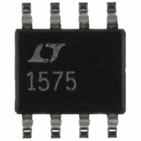
LT1575CS8 Linear Technology, LT1575CS8 Datasheet - Page 3

LT1575CS8
Manufacturer Part Number
LT1575CS8
Description
IC LDO REG ADJ SINGLE 8-SOIC
Manufacturer
Linear Technology
Type
Positive Adjustabler
Datasheet
1.LT1575CN8-2.8.pdf
(20 pages)
Specifications of LT1575CS8
Number Of Outputs
1
Voltage - Output
Adjustable
Current - Supply
12mA
Voltage - Input
10 ~ 20 V
Operating Temperature
0°C ~ 70°C
Package / Case
8-SOIC (3.9mm Width)
Lead Free Status / RoHS Status
Contains lead / RoHS non-compliant
Available stocks
Company
Part Number
Manufacturer
Quantity
Price
Part Number:
LT1575CS8
Manufacturer:
LINEAR/凌特
Quantity:
20 000
Part Number:
LT1575CS8#TR
Manufacturer:
LT/凌特
Quantity:
20 000
Part Number:
LT1575CS8-1.5#TRPBF
Manufacturer:
LINEAR/凌特
Quantity:
20 000
Part Number:
LT1575CS8-2.8
Manufacturer:
LINEAR/凌特
Quantity:
20 000
Part Number:
LT1575CS8-2.8#PBF
Manufacturer:
LINEAR/凌特
Quantity:
20 000
ELECTRICAL CHARACTERISTICS
T
SYMBOL
I
V
V
I
I
A
V
V
The
temperature range.
Note 1: Absolute Maximum Ratings are those values beyond which the life
of the device may be impaired.
Note 2: T
dissipation P
Q
FB
OUT
A
FB
OUT
VOL
OL
OH
= 25 C, V
LT1575CN8: T
LT1575CS8: T
LT1577CS: T
denotes specifications which apply over the full operating
J
is calculated from the ambient temperature T
D
IN
PARAMETER
Supply Current
LT1575 Reference Voltage
LT1575-1.5 Output Voltage
LT1575-2.8 Output Voltage
LT1575-3.3 Output Voltage
LT1575-3.5 Output Voltage
LT1575-5 Output Voltage
Line Regulation
FB Input Bias Current
OUT Divider Current
LT1575 Large-Signal Voltage Gain
LT1575-1.5 Large-Signal Voltage Gain
LT1575-2.8 Large-Signal Voltage Gain
LT1575-3.3 Large-Signal Voltage Gain
LT1575-3.5 Large-Signal Voltage Gain
LT1575-5 Large-Signal Voltage Gain
GATE Output Swing Low (Note 3)
GATE Output Swing High
IPOS + INEG Supply Current
Current Limit Threshold Voltage
Current Limit Threshold Voltage
Line Regulation
SHDN Sink Current
SHDN Source Current
SHDN Low Clamp Voltage
SHDN High Clamp Voltage
SHDN Threshold Voltage
SHDN Threshold Hysteresis
according to the following formulas:
J
= 12V, GATE = 6V, IPOS = INEG = 5V, SHDN = 0.75V unless otherwise noted.
J
J
= T
= T
= T
A
A
A
+ (P
+ (P
+ (P
D
D
D
• 100 CW)
• 130 CW)
• 100 CW)
A
and power
CONDITIONS
10V V
FB = V
OUT = V
V
V
V
V
V
V
I
I
3V IPOS 20V
3V IPOS 20V
Current Flows Into Pin
Current Flows Out of Pin
GATE
GATE
GATE
GATE
GATE
GATE
GATE
GATE
= 0mA
= 0mA
FB
= 3V to 10V
= 3V to 10V
= 3V to 10V
= 3V to 10V
= 3V to 10V
= 3V to 10V
IN
OUT
20V
Because the LT1577 consists of two regulators in the package, the total
LT1577 power dissipation must be used for its junction temperature
calculation. The total LT1577 P
Note 3: The V
3V – V
OUT
.
GS(th)
of the external MOSFET must be greater than
V
IN
– 0.6
– 1.0
– 0.6
– 1.0
– 0.6
– 1.0
– 0.6
– 1.0
– 0.6
– 1.0
– 0.6
– 1.0
1.50
1.18
MIN
0.5
0.3
2.5
– 8
69
67
60
60
60
56
42
37
50
D
5
– 1.6
= P
D
(Regulator 1) + P
LT1575/LT1577
V
– 0.20
1.210
1.210
1.500
1.500
2.800
2.800
3.300
3.300
3.500
3.500
5.000
5.000
0.625
– 0.6
0.01
1.85
1.21
TYP
IN
– 15
100
1.0
2.5
5.0
0.1
12
84
82
76
75
74
71
50
50
– 1
– 0.50
1.240
MAX
– 4.0
0.03
0.25
2.20
– 23
150
D
0.6
1.0
0.6
1.0
0.6
1.0
0.6
1.0
0.6
1.0
0.6
1.0
1.5
3.0
1.0
8.0
58
19
63
(Regulator 2).
UNITS
3
%/V
%/V
mA
mA
mA
mV
mV
mV
dB
dB
dB
dB
dB
dB
%
%
%
%
%
%
%
%
%
%
%
%
A
V
V
A
A
V
V
V


