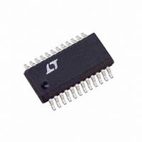
LTC3722EGN-1#PBF Linear Technology, LTC3722EGN-1#PBF Datasheet - Page 18

LTC3722EGN-1#PBF
Manufacturer Part Number
LTC3722EGN-1#PBF
Description
IC CTLR PWM CURRENT-MODE 24SSOP
Manufacturer
Linear Technology
Datasheet
1.LTC3722EGN-1PBF.pdf
(28 pages)
Specifications of LTC3722EGN-1#PBF
Pwm Type
Current Mode, Full Bridge
Number Of Outputs
1
Frequency - Max
1MHz
Duty Cycle
98.5%
Voltage - Supply
3.8 V ~ 10.3 V
Buck
No
Boost
No
Flyback
No
Inverting
No
Doubler
No
Divider
Yes
Cuk
No
Isolated
Yes
Operating Temperature
-40°C ~ 85°C
Package / Case
24-SSOP
Frequency-max
1MHz
Lead Free Status / RoHS Status
Lead free / RoHS Compliant
Available stocks
Company
Part Number
Manufacturer
Quantity
Price
LTC3722-1/LTC3722-2
operaTion
3. Slope compensation is required for most peak current
mode controllers in order to prevent subharmonic
oscillation of the current control loop. In general, if the
system duty cycle exceeds 50% in a fixed frequency,
continuous current mode converter, an unstable con-
dition exists within the current control loop. Any
perturbation in the current signal is amplified by the
PWM modulator resulting in an unstable condition.
Some common manifestations of this include alternate
pulse nonuniformity and pulse width jitter. Fortunately,
this can be addressed by adding a corrective slope to
the current sense signal or by subtracting the same
slope from the current command signal (error am-
plifier output). In theory, the current doubler output
configuration does not require slope compensation
since the output inductor duty cycles only approach
50%. However, transient conditions can momentarily
cause higher duty cycles and therefore, the possibility
for unstable operation.
The exact amount of required slope compensation is
easily programmed by the LTC3722-1/LTC3722-2 with
the addition of a single external resistor (see Figure 9).
The LTC3722-1/LTC3722-2 generates a current that
is proportional to the instantaneous voltage on C
(33µA/V(C
approximately 74µA and is output from the CS pin. A
resistor connected between CS and the external current
sense resistor sums in the required amount of slope
compensation. The value of this resistor is dependent
on several factors including minimum V
ing frequency, current sense resistor value and output
inductor value. An illustrative example with the design
equation for current doubler secondary follows.
Example:
V
V
I
L = 2.2µH
OUT
IN
OUT
= 36V to 72V
= 40A
= 3.3V
T
)). Thus, at the peak of C
T
IN
, this current is
, V
OUT
, switch-
T
,
Transformer turns ratio (N) =
R
R
to account for tolerances in I
R
V
f
=
f
SW
SW
CS
SLOPE
IN MIN
2
SL
3 3
(
.
= 0.05Ω
O O PE
=
C
=
T
V
300
150
= 338Ω, choose the next higher standard value
)
Figure 9. Slope Compensation Circuitry
•
=
•
2
V
kHz i e transformer f
kHz
( •
O
2
DC
• .
LTC3722
•
33k
, . .,
2 2 H H
I =
V
MAX
( • •
OUT
2
V(C
µ
33k
T
L f
)
)
•
0 05
=
300
.
SW
CS
SLOPE
ADDED
5
R
CURRENT SENSE
k
CS
SLOPE
WAVEFORM
•
•
R
74
SLOPE
74
µA N
, R
µA
• )
CS
=
•
, N and L.
5
372212 F09
R
BRIDGE
CURRENT
CS
372212fa


