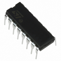
SG2525AN STMicroelectronics, SG2525AN Datasheet - Page 4

SG2525AN
Manufacturer Part Number
SG2525AN
Description
IC MODULATOR REG PULSE 16 DIP
Manufacturer
STMicroelectronics
Type
Pulse Width Modulator Controllerr
Specifications of SG2525AN
Pwm Type
Voltage Mode
Number Of Outputs
2
Frequency - Max
500kHz
Duty Cycle
49%
Voltage - Supply
8 V ~ 35 V
Buck
No
Boost
No
Flyback
No
Inverting
No
Doubler
No
Divider
No
Cuk
No
Isolated
No
Operating Temperature
-25°C ~ 85°C
Package / Case
16-DIP (0.300", 7.62mm)
Frequency-max
500kHz
Output Voltage
5.15 V
Input Voltage
8 V to 35 V
Switching Frequency
500 KHz
Operating Temperature Range
- 25 C to + 85 C
Mounting Style
Through Hole
Duty Cycle (max)
49 %
Common Mode Rejection Ratio
75
Current, Input Bias
1 μA
Current, Input Offset
1 μA
Current, Output
0 to 100 mA (Steady State), 0 to 400 mA (Peak)
Current, Supply
14 mA
Frequency, Oscillator
400 kHz
Package Type
DIP-16
Power Dissipation
1000 mW
Regulation, Line
10 mV
Regulation, Load
20 mV
Temperature, Operating, Range
-25 to +85 °C
Time, Fall
50 ns
Time, Rise
100 ns
Transconductance
1.5
Voltage, Gain
75 dB
Voltage, Input
35 V
Voltage, Noise
40 μV
Voltage, Offset
0.5 mV
Voltage, Output
5.1 V
Voltage, Output, High
18 V
Voltage, Output, Low
1 V
Voltage, Supply
4.5 to 35 V
Voltage, Supply, Rejection Ratio
60 dB
Lead Free Status / RoHS Status
Lead free / RoHS Compliant
Other names
497-2038-5
Available stocks
Company
Part Number
Manufacturer
Quantity
Price
SG2525A-SG3525A
ELECTRICAL CHARACTERISTICS (continued)
* These parameters, although guaranteed over the recommended operating conditions, are not 100 % tested in production.
.
4/12
PWM COMPARATOR
SHUTDOWN SECTION
OUTPUT DRIVERS (each output) (V
TOTAL STANDBY CURRENT
Symbol
Tested at f
f =
DC transconductance (g
from pin 9 to ground. The minimum g
t
t
I
I
*
*
r
f
C
s
*
*
C
T
(0.7 R
osc
Minimum Duty-cycle
Maximum Duty-cycle
Input Threshold
Input Bias Current
Soft Start Current
Soft Start Low Level
Shutdown Threshold
Shutdown Input Current V
Shutdown Delay
Output Low Level
Output High Level
Under-Voltage Lockout
Collector Leakage
Rise Time
Fall Time
Supply Current
= 40 KHz (R
1
T
+ 3 R
Parameter
D
)
M
) relates to DC open-loop voltage gain (G
T
= 3.6 K , C
M
specification is used to calculate minimum G
T
= 10nF, R
Zero Duty-cycle
Maximum Duty-cycle
V
V
To outputs, V
T
V
I
I
I
I
V
V
C
C
C
sink
sink
source
source
SD
SD
j
SD
SD
comp
C
L
L
= 20 V)
= 25 C
= 1 nF, T
= 1 nF, T
= 35 V
Test Conditions
= 20 mA
= 100 mA
= 0 V, V
= 2.5 V
= 2.5 V
= 2.5 V T
D
= 20 mA
= 100 mA
and V
= 0 ). Approximate oscillator frequency is defined by :
V
i
= 35 V
ss
SS
j
j
j
SS
= High
= 25 C
= 25 C
= 25 C
= 0 V
= 5.1 V
v
) according to the following equation : G
Min.
0.7
0.6
45
25
18
17
6
SG2525A
v
when the error amplifier output is loaded.
Typ.
0.05
100
0.9
3.3
0.4
0.8
0.4
0.2
0.2
49
50
19
18
50
14
1
7
Max.
200
600
300
3.6
0.7
0.5
0.4
80
20
0
1
1
1
2
8
Min.
0.7
0.6
25
18
17
45
v
6
= g
SG3525A
M
R
Typ.
0.05
100
L
0.9
3.3
0.4
0.8
0.4
0.2
0.2
49
50
19
18
50
14
where R
1
7
Max.
200
600
300
3.6
0.7
0.5
0.4
L
80
20
0
1
1
1
2
8
is the resistance
Unit
mA
mA
ns
ns
%
%
V
V
V
V
V
V
V
V
V
A
A
A
s


