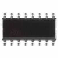
L5993D STMicroelectronics, L5993D Datasheet - Page 10

L5993D
Manufacturer Part Number
L5993D
Description
IC PWM CONTROLLER 16 SOIC
Manufacturer
STMicroelectronics
Datasheet
1.L5993D.pdf
(22 pages)
Specifications of L5993D
Pwm Type
Current Mode
Number Of Outputs
1
Frequency - Max
1MHz
Duty Cycle
85%
Voltage - Supply
11 V ~ 20 V
Buck
No
Boost
No
Flyback
Yes
Inverting
No
Doubler
No
Divider
No
Cuk
No
Isolated
Yes
Operating Temperature
0°C ~ 105°C
Package / Case
16-SOIC (3.9mm Width)
Frequency-max
1MHz
Lead Free Status / RoHS Status
Contains lead / Request inventory verification
Other names
497-2387-5
Available stocks
Company
Part Number
Manufacturer
Quantity
Price
L5993
Pin 5. VFB (Error Amplifier Inverting Input). The
feedback signal is applied to this pin and is com-
pared to the E/A internal reference (2.5V). The
E/A output generates the control voltage which
fixes the duty cycle.
The E/A features high gain-bandwidth product,
which allows to broaden the bandwidth of the
overall control loop, high slew-rate and current ca-
pability, which improves its large signal behavior.
Usually the compensation network, which stabi-
lizes the overall control loop, is connected be-
tween this pin and COMP (pin 6).
Pin 6. COMP (Error Amplifier Output). Usually,
this pin is used for frequency compensation and
the relevant network is connected between this
pin and VFB (pin 5). Compensation networks to-
wards ground are not possible since the L5993
E/A is a voltage mode amplifier (low output im-
pedance). See application ideas for some exam-
ple of compensation techniques.
Pin 7. SS (Soft-Start). At device start-up, a ca-
pacitor (Css) connected between this pin and
SGND (pin 12) is charged by an internal current
generator, ISSC, up to about 7V. During this
ramp, the E/A output is clamped by the voltage
across Css itself and allowed to rise linearly, start-
ing from zero, up to the steady-state value im-
posed by the control loop. The maximum time in-
terval during which the E/A is clamped, referred to
as soft-start time, is approximately:
where R
13) and I
through R
Figure 24. Hiccup mode operation.
10/22
FAULT
I
I
OUT
SEN
SS
0.5V
T
5V
sense
ss
Qpk
sense
3 R
is the current sense resistor (see pin
is the switch peak current (flowing
), which depends on the output
sense
I
SSC
I
Qpk
C
ss
(6)
T
hic
SHORT
Figure 23. Regulation characteristic and re-
load. Usually, C
der of milliseconds.
As mentioned before, the soft-start intervenes
also in case of severe overload or short circuit on
the output. Referring to fig. 23, pulse-by-pulse
current limitation is somehow effective as long as
the ON-time of the power switch can be reduced
(from A to B). After the minimum ON-time is
reached (from B onwards) the current is out of
control.
To prevent this risk, a comparator trips an over-
current handling procedure, named ’hiccup’ mode
operation, when a voltage above 1.2V (point C) is
detected on current sense input (ISEN, pin 13).
Basically, the IC is turned off and then soft-started
as long as the fault condition is detected. As a re-
sult, the operating point is moved abruptly to D,
creating a foldback effect. Fig. 24 illustrates the
operation.
The oscillation frequency appearing on the soft-
V
T
OUT
ON
D97IN495
D.C.M.
lated quantities
SS
C.C.M.
I
D98IN986
SHORT
is selected for a T
D
I
A
OUT(max)
B
C
7V
SS
time
I
in the or-
OUT
1-2 ·I
I
I
T
Qpk(max)
Qpk
ON(min)
Qpk


