MC34060APG ON Semiconductor, MC34060APG Datasheet - Page 5
MC34060APG
Manufacturer Part Number
MC34060APG
Description
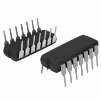
IC CTLR SMPS PWM FXD FREQ 14DIP
Manufacturer
ON Semiconductor
Datasheet
1.MC34060APG.pdf
(16 pages)
Specifications of MC34060APG
Pwm Type
Voltage Mode
Number Of Outputs
1
Frequency - Max
200kHz
Duty Cycle
100%
Voltage - Supply
7 V ~ 40 V
Buck
Yes
Boost
Yes
Flyback
Yes
Inverting
Yes
Doubler
No
Divider
No
Cuk
No
Isolated
Yes
Operating Temperature
0°C ~ 70°C
Package / Case
14-DIP (0.300", 7.62mm)
Frequency-max
200kHz
Topology
Flyback
Output Voltage
30 V
Output Current
200 mA
Switching Frequency
200 KHz
Duty Cycle (max)
96 %
Operating Supply Voltage
15 V
Maximum Operating Temperature
+ 70 C
Minimum Operating Temperature
0 C
Fall Time
40 ns
Mounting Style
Through Hole
Rise Time
100 ns
Synchronous Pin
No
Lead Free Status / RoHS Status
Lead free / RoHS Compliant
Other names
MC34060APGOS
Available stocks
Company
Part Number
Manufacturer
Quantity
Price
Company:

Part Number:
MC34060APG
Manufacturer:
LEACH
Quantity:
35


Description
modulation control circuit, incorporating the primary
building blocks required for the control of a switching power
supply (see Figure 1). An internal−linear sawtooth oscillator
is frequency−programmable by two external components,
R
determined by:
T
The MC34060A is a fixed−frequency pulse width
and C
Dead-Time
T
R
Control
. The approximate oscillator frequency is
For more information refer to Figure 3.
T
C
T
f
Dead-Time Control
osc
6
5
4
Feedback/P.W.M.
Comparator
^
Capacitor C
Error Amp
1
1
Output Q
R
Emitter
T
1.2
2
• C
T
+
-
1
T
,
1
≈ 0.7mA
Oscillator
0.12V
0.7V
Comparator Input
Feedback/PWM
This device contains 46 active transistors.
3
Figure 2. Timing Diagram
Figure 1. Block Diagram
http://onsemi.com
-
+
-
+
Comparator
Dead-Time
Comparator
PWM.
2
5
+
-
13
Error Amp
comparison of the positive sawtooth waveform across
capacitor C
enabled only during that portion of time when the sawtooth
voltage is greater than the control signals. Therefore, an
increase in control−signal amplitude causes a corresponding
linear decrease of output pulse width. (Refer to the Timing
Diagram shown in Figure 2.)
2
Output pulse width modulation is accomplished by
Undervoltage
14
Lockout
T
to either of two control signals. The output is
-
+
Reference
Regulator
7
GND
V
TH
Q1
10
12
8
9
Collector
Ref Out
Emitter
V
CC
Related parts for MC34060APG
Image
Part Number
Description
Manufacturer
Datasheet
Request
R

Part Number:
Description:
ON Semiconductor [VOLTAGE REGULATOR]
Manufacturer:
ON Semiconductor
Datasheet:
Part Number:
Description:
357-036-542-201 CARDEDGE 36POS DL .156 BLK LOPRO
Manufacturer:
ON Semiconductor
Datasheet:
Part Number:
Description:
357-036-542-201 CARDEDGE 36POS DL .156 BLK LOPRO
Manufacturer:
ON Semiconductor
Datasheet:
Part Number:
Description:
357-036-542-201 CARDEDGE 36POS DL .156 BLK LOPRO
Manufacturer:
ON Semiconductor
Datasheet:
Part Number:
Description:
357-036-542-201 CARDEDGE 36POS DL .156 BLK LOPRO
Manufacturer:
ON Semiconductor
Datasheet:
Part Number:
Description:
357-036-542-201 CARDEDGE 36POS DL .156 BLK LOPRO
Manufacturer:
ON Semiconductor
Datasheet:
Part Number:
Description:
357-036-542-201 CARDEDGE 36POS DL .156 BLK LOPRO
Manufacturer:
ON Semiconductor
Datasheet:
Part Number:
Description:
357-036-542-201 CARDEDGE 36POS DL .156 BLK LOPRO
Manufacturer:
ON Semiconductor
Datasheet:
Part Number:
Description:
357-036-542-201 CARDEDGE 36POS DL .156 BLK LOPRO
Manufacturer:
ON Semiconductor
Datasheet:
Part Number:
Description:
357-036-542-201 CARDEDGE 36POS DL .156 BLK LOPRO
Manufacturer:
ON Semiconductor
Datasheet:
Part Number:
Description:
357-036-542-201 CARDEDGE 36POS DL .156 BLK LOPRO
Manufacturer:
ON Semiconductor
Datasheet:
Part Number:
Description:
Manufacturer:
ON Semiconductor
Datasheet:
Part Number:
Description:
Manufacturer:
ON Semiconductor
Datasheet:
Part Number:
Description:
Manufacturer:
ON Semiconductor
Datasheet: