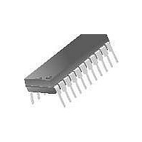
KA3511DS Fairchild Semiconductor, KA3511DS Datasheet

KA3511DS
Specifications of KA3511DS
Available stocks
Related parts for KA3511DS
KA3511DS Summary of contents
Page 1
AN4003 PC POWER SUPPLY DESIGN WITH KA3511 Sang-Tae Im 1. GENERAL DESCRIPTION The KA3511 is a fixed-frequency improved-performance pulse-width modulation control circuit with complete housekeeping circuitry for use in the secondary side of SMPS (Switched mode power supply). It contains ...
Page 2
ORDERING INFORMATION Device Package KA3511 22 DIP FEATURES • Complete PWM control and house keeping circuitry • Few external components • Precision voltage reference trimmed to 2% • Dual output for push-pull operation • Each output TR for 200mA sink ...
Page 3
PIN DESCRIPTION Pin No. Name I Supply voltage CC 2 COMP O E/A output 3 E/A(-) I E/A (-) input 4 E/A(+) I E/A (+) input 5 TREM – Remote on/off delay 6 REM I Remote ...
Page 4
Pin No. Name 1 V Supply voltage. Operating range is 14V~30V COMP Error amplifier output connected to non-inverting input of pulse width modulator comparator. 3 E/A(-) Error amplifier inverting input. Its reference voltage is always ...
Page 5
ABSOLUTE MAXIMUM RATINGS Characteristic Supply voltage Collector output voltage Collector output current Power dissipation Operating temperature Storage temperature TEMPERATURE CHARACTERISTICS Characteristic Temperature coefficient of Vref (-25 °C<Ta<85°C) Symbol Value ...
Page 6
ELECTRICAL CHARACTERISTICS (V Characteristic REFERENCE SECTION Reference output voltage Line regulation Load regulation Temperature coefficient of Vref Short-circuit output current OSCILLATOR SECTION Oscillation frequency Frequency change with (1) temperature DEAD TIME CONTROL SECTION Input bias current Maximum duty voltage ...
Page 7
ELECTRICAL CHARACTERISTICS (continued) Characteristic Over voltage protection for 5V Over voltage protection for 12V Input threshold voltage for PT Under voltage protection for 3.3V Under voltage protection for 5V Under voltage protection for 12V Charging current for UVP delay ...
Page 8
BLOCK DESCRIPTION & APPLICATION INFORMATIONS 6.1 OSCILLATOR BLOCK The KA3511 is a fixed-frequency pulse width modulation control circuit. An internal-linear sawtooth oscillator is frequency-programmable by two external components, R quency is determined by Figure 2. Oscillator Frequency vs. Timing ...
Page 9
The control signals are external inputs that can be fed into the dead-time control, the error amplifier inputs, or the feedback input. The dead-time control comparator has an effective 120mV input off- set which limits the minimum output dead time. ...
Page 10
DEADTIME CONTROL for SOFT-START Deadtime control for soft-start makes a power supply output rising time (Typ. 15ms) to reduce out- put ringing voltage for 3.3V, 5V, and 12V. If output rising time is too fast, output ringing voltage reaches ...
Page 11
So Output Duty Ratio will change from the minimum duty ratio to the maximum duty ratio. Also, if the remote voltage is high, the deadtime control voltage will keep 3V (=3mA xR2 ( the internal 3mA current source ...
Page 12
OVP BLOCK OVP function is simply realized by connecting Pin13, Pin14, Pin15 to each secondary output. R1 are internal resistors of the IC. Each OVP level is determined by resistor ratio and the typical ...
Page 13
UVP BLOCK The KA3511 has UVP functions for +3.3V, +5V, +12V Outputs. The block is made up of three input comparators. Each UVP level is determined by resistor ratio and the typical values are 2.3V/4V/ 10V. UVP Detecting voltage ...
Page 14
REMOTE ON/OFF & DELAY BLOCK Figure 9. Remote ON/OFF Delay Block Remote ON/OFF section is controlled by a microprocessor high signal is supplied to the remote ON/OFF input (Pin6), the output of COMP6 becomes high status. The ...
Page 15
R/S FLIP FLOP (LATCH) BLOCK OVP+ SET Low Low Low Low High High High Low There is a R-S F/F (Latch) circuit for shutdown operation in the KA3511. R-S F/F (Latch) is con- trolled by OVP, UVP, and some ...
Page 16
POWER GOOD SIGNAL GENERATOR Power good signal generator curcuits generate “ON & OFF” signal depending on the status of out- put voltage to prevent the malfunctions of following systems like microprocessor and etc. from unstable outputs at power on ...
Page 17
Considering the lightning surge and noise, there are two types of protections. One is a few sec- onds delay between TPG and PG for safe operation and another is some noise margin of Pin10. Noise_Margin_of_T = V10(max) – Vth(L) = ...
Page 18
HOUSE KEEPING CIRCUIT Using the KA3511 requires few external components to accomplish a complete housekeeping cir- cuits for SMPS. 18 Rev C, November 1999 ...
Page 19
TYPICAL CHARACTERISTICS 19 Rev C, November 1999 ...
Page 20
Rev C, November 1999 ...
Page 21
Rev C, November 1999 ...
Page 22
Rev C, November 1999 ...
Page 23
PACKAGE DIMENSION 9.14 0.20 0.360 0.008 1 11 10.16 0.400 22-DIP-400 22 12 3.81 0.20 0.150 0.008 5.08 MAX 0.200 23 0.51 MIN 0.020 3.40 0.30 0.134 0.012 Rev C, November 1999 ...
Page 24
EXPERIMENTAL RESULT Figure 12. Rising Time of +5Vdc Output Voltage Figure 13. PG Signal Delay Time 24 Rev C, November 1999 ...
Page 25
Figure 14. Power Down Warning Figure 15. No Load Protection 25 Rev C, November 1999 ...
Page 26
Figure 16. Vcc, +5Vdc Output vs. PG Signal (High) Figure 16. Vcc, +5Vdc Output vs. PG Signal (Low) 26 Rev C, November 1999 ...
Page 27
APPLICATION CIRCUIT Reference 1. Power Electronics by Marvin J. Fisher 2. Principles Of Power Electronics by Kassakian AUTHOR: Sang-Tae Im: P-IC Application Team Tel. 82-32-680-1275 Fax. 82-32-680-1317 E-mail. sangtae.im@Fairchildsemi.co. Rev C, November 1999 ...
Page 28
... TRADEMARKS The following are registered and unregistered trademarks Fairchild Semiconductor owns or is authorized to use and is not intended exhaustive list of all such trademarks. ACEx™ CoolFET™ CROSSVOLT™ CMOS FACT™ FACT Quiet Series™ ® FAST FASTr™ GTO™ ...


