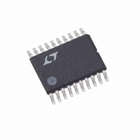
LT3570IFE#PBF Linear Technology, LT3570IFE#PBF Datasheet - Page 9

LT3570IFE#PBF
Manufacturer Part Number
LT3570IFE#PBF
Description
IC PWM BUCK BST DIV CM 20TSSOP
Manufacturer
Linear Technology
Datasheet
1.LT3570EFEPBF.pdf
(20 pages)
Specifications of LT3570IFE#PBF
Topology
Step-Down (Buck) (1), Step-Up (Boost) (1), Linear (LDO) (1)
Function
Automotive
Number Of Outputs
3
Frequency - Switching
500kHz ~ 2.1MHz
Voltage/current - Output 1
Adj to 0.8V, 1.5A
Voltage/current - Output 2
Adj to 0.8V, 1.5A
Voltage/current - Output 3
Controller
W/led Driver
No
W/supervisor
No
W/sequencer
No
Voltage - Supply
2.5 V ~ 36 V
Operating Temperature
-40°C ~ 125°C
Mounting Type
*
Package / Case
20-TSSOP Exposed Pad, 20-eTSSOP, 20-HTSSOP
Frequency-max
2.75MHz
Duty Cycle
95%
Pwm Type
Current Mode
Buck
Yes
Boost
Yes
Flyback
No
Inverting
No
Doubler
No
Divider
Yes
Cuk
No
Isolated
No
Lead Free Status / RoHS Status
Lead free / RoHS Compliant
Available stocks
Company
Part Number
Manufacturer
Quantity
Price
The LT3570 is a constant frequency, current mode, buck
converter and boost converter with an NPN LDO regula-
tor. Operation can be best understood by referring to the
Block Diagram.
If all of the SHDN pins are held low, the LT3570 is shut
down and draws zero quiescent current. When any of the
pins exceed 1.4V the internal bias circuits turn on. Each
regulator will only begin regulating when its corresponding
SHDN pin is pulled high.
Each switching regulator controls the output voltage in
a similar manner. The operation of the switchers can be
understood by looking at the boost regulator. A pulse
from the oscillator sets the RS fl ip-fl op A4 and turns on
the internal NPN bipolar power switch Q1. Current in Q1
and the external inductor L1 begins to increase. When
this current exceeds a level determined by the voltage at
V
in L1 fl ows through the external Schottky diode D1 and
begins to decrease. The cycle begins again at the next
pulse from the oscillator. In this way, the voltage on the
OPERATION
C1
, comparator A3 resets A4, turning off Q1. The current
V
output. The internal error amplifi er A1 regulates the output
voltage by continually adjusting the V
threshold for switching on the V
750mV and an active clamp of 1.15V limits the output
current. The soft-start capacitor C6A allows the part to
slowly start up by ramping the internal reference.
The driver for the buck regulator can operate from either
V
diode are used to generate a voltage at the BOOST pin that
is higher than the input supply. This allows the driver to
saturate the internal bipolar NPN power switch for effi cient
operation. The driver for the boost regulator is operated
from V
The BIAS pin allows the internal circuitry to draw its
current from a lower voltage supply than the input. This
reduces power dissipation and increases effi ciency. If the
voltage on the BIAS pin falls below 2.5V, then the LT3570
quiescent current will fl ow from V
C1
IN2
pin controls the current through the inductor to the
or from the BOOST pin. An external capacitor and
IN1
.
C1
IN2
pin is approximately
.
C1
pin voltage. The
LT3570
3570fb
9


