SG3526BN Microsemi Analog Mixed Signal Group, SG3526BN Datasheet - Page 3
SG3526BN
Manufacturer Part Number
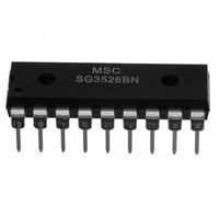
SG3526BN
Description
IC PWM POWER SUPPLY SW 18DIP
Manufacturer
Microsemi Analog Mixed Signal Group
Datasheet
1.SG2526BN.pdf
(9 pages)
Specifications of SG3526BN
Pwm Type
Voltage Mode
Number Of Outputs
2
Frequency - Max
500kHz
Duty Cycle
49%
Voltage - Supply
8 V ~ 35 V
Buck
Yes
Boost
No
Flyback
No
Inverting
No
Doubler
No
Divider
No
Cuk
No
Isolated
No
Operating Temperature
0°C ~ 70°C
Package / Case
18-DIP
Frequency-max
500kHz
Lead Free Status / RoHS Status
Lead free / RoHS Compliant
Other names
SG3526BNR
SG3526BNR
SG3526BNR
Available stocks
Company
Part Number
Manufacturer
Quantity
Price


Rev 1.1a
Copyright
ELECTRICAL CHARACTERISTICS
Note 3. I
Note 4. F
Note 5. V
Note 6. V
Oscillator Section
Initial Accuracy
Voltage Stability
Temperature Stability
Minimum Frequency
Maximum Frequency
Sawtooth Peak Voltage
Sawtooth Valley Voltage
SYNC Pulse Width
Error Amplifier Section
Input Offset Voltage
Input Bias Current
Input Offset Current
DC Open Loop Gain
High Output Voltage
Low Output Voltage
Common Mode Rejection
Supply Voltage Rejection
PWM Comparator Section
Minimum Duty Cycle
Maximum Duty Cycle
Digital Ports (SYNC, SHUTDOWN, and RESET)
HIGH Output Voltage
LOW Output Voltage
HIGH Input Current
LOW Input Current
SHUTDOWN Delay to Output
Current Limit Comparator Section
Sense Voltage
Input Bias Current
Delay to Output
Soft-Start Section
Error Clamp Voltage
C
Output Drivers (each output)
HIGH Output Voltage
LOW Output Voltage
Collector Leakage
Rise Time
Fall Time
Power Consumption Section
Standby Current
S
Charging Current
1994
L
OSC
CM
CM
= 0mA
= 0 to 5.2V
= 0 to 12V
= 40KHz (R
Parameter
(Note 9)
(Note 4)
(Note 9)
T
(Note 9)
= 4.12K
(Note 5)
(Note 4)
(Note 7)
(Note 8)
1%, C
T
V
Over Operating T
R
R
V
V
R
R
R
V
V
R
V
V
V
I
I
V
V
(Note 6)
R
RESET = 0.4V
RESET = 2.4V
I
I
I
I
V
C
C
SHUTDOWN = 0.4V
SOURCE
SINK
(Note9)
SOURCE
SOURCE
SINK
SINK
T
J
IN
IN
IN
PIN1
PIN2
IN
COMPENSATION
COMPENSATION
IH
IL
C
T
T
L
S
L
S
S
L
L
= .01 F 1%, R
= 25 C
= 150K , C
= 2K , C
= 2.0K to V
= 40V
= 1000pF
= 1000pF
= 0.4V
(continued)
= 8 to 35V
= 35V
= 8V
= 8V to 35V
= 2.4V
= 3.6mA
= 20mA
= 100mA
10M
2K
- V
- V
2K
50
= 40 A
= 20mA
= 100mA
PIN2
PIN1
T
= 0.4V
= 3.6V
150mV, I
150mV, I
= 470pF
Test Conditions
T
REF
= 20 F
D
J
= 0 )
SOURCE
SINK
= 100 A
3
= 100 A
Note 7. V
Note 8. V
Note 9. These parameters, although guaranteed over the recom-
mended operating conditions, are not tested in production.
C
IN
SG1526B/SG2526B/SG3526B
= 15V
= 35V
Min. Typ. Max. Min. Typ. Max.
12.5
SG1526B/2526B
500
2.5
0.5
2.4
3.6
64
70
66
45
90
50
12
-350
-125
-225
13.5
100
100
0.5
3.0
1.0
1.0
4.2
0.2
0.2
0.1
0.2
1.2
0.3
0.1
35
72
94
80
49
13
50
18
-3
7
2
4
3
11861 Western Avenue
-1000
-200
-360
0.15
100
200
110
400
0.4.
150
150
1.0
1.0
3.5
1.1
0.4
0.4
-10
0.3
0.4
10
30
2
5
0
2
8
12.5
(714) 898-8121
500
2.5
0.5
3.6
2.4
60
70
66
45
80
50
12
SG3526B
-350
-125
-225
13.5
100
100
0.5
3.0
1.0
1.0
4.2
0.2
0.2
0.1
0.2
1.2
0.3
0.1
35
72
94
80
49
13
50
18
-3
3
2
4
3
Garden Grove, CA 92841
-2000
-200
-360
0.15
200
200
120
400
0.4.
150
150
-10
1.0
1.0
3.5
1.1
0.4
0.4
0.3
0.4
10
30
FAX: (714) 893-2570
5
2
0
2
8
Units
KHz
mV
mV
mA
Hz
nA
nA
dB
dB
dB
ns
ns
%
%
%
%
%
V
V
V
V
V
V
V
V
V
V
V
A
A
A
A
A
s
s
s
Related parts for SG3526BN
Image
Part Number
Description
Manufacturer
Datasheet
Request
R

Part Number:
Description:
IC USB LINE TERM EMI/ESD SC70-6
Manufacturer:
Microsemi Analog Mixed Signal Group
Datasheet:

Part Number:
Description:
IC USB LINE TERM EMI/ESD SC70-6
Manufacturer:
Microsemi Analog Mixed Signal Group
Datasheet:

Part Number:
Description:
IC TERM SCSI 9LINE MODE 24TSSOP
Manufacturer:
Microsemi Analog Mixed Signal Group
Datasheet:

Part Number:
Description:
IC TERM SCSI 9LINE MODE 28TSSOP
Manufacturer:
Microsemi Analog Mixed Signal Group
Datasheet:

Part Number:
Description:
IC TERM SCSI 9LINE LVD 24TSSOP
Manufacturer:
Microsemi Analog Mixed Signal Group
Datasheet:
Part Number:
Description:
IC TERM SCSI 9LINE MODE 36QSOP
Manufacturer:
Microsemi Analog Mixed Signal Group
Datasheet:

Part Number:
Description:
IC USB LINE TERM EMI/ESD SOT23-6
Manufacturer:
Microsemi Analog Mixed Signal Group
Datasheet:

Part Number:
Description:
IC USB LINE TERM EMI/ESD SOT23-6
Manufacturer:
Microsemi Analog Mixed Signal Group
Datasheet:

Part Number:
Description:
IC USB EMI FLTR ESD PROT SOT23-6
Manufacturer:
Microsemi Analog Mixed Signal Group
Part Number:
Description:
IC USB LINE TERM EMI/ESD SOT23-6
Manufacturer:
Microsemi Analog Mixed Signal Group
Datasheet:
Part Number:
Description:
IC AMP AUDIO PWR 10W STER 44SSOP
Manufacturer:
Microsemi Analog Mixed Signal Group
Datasheet:

Part Number:
Description:
IC CHARGER BATT USB LI-ION 20MLP
Manufacturer:
Microsemi Analog Mixed Signal Group
Datasheet:

Part Number:
Description:
IC LED DRIVER LINEAR 6-MLP
Manufacturer:
Microsemi Analog Mixed Signal Group
Datasheet:

Part Number:
Description:
IC LED DRIVR WT/CLR BCKLGT 8-MLP
Manufacturer:
Microsemi Analog Mixed Signal Group
Datasheet:

Part Number:
Description:
IC LED DRVR WT/CLR BCKLGT 8-MSOP
Manufacturer:
Microsemi Analog Mixed Signal Group
Datasheet: