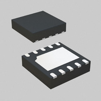
IR3624MTRPBF International Rectifier, IR3624MTRPBF Datasheet - Page 14

IR3624MTRPBF
Manufacturer Part Number
IR3624MTRPBF
Description
IC CTRLR PWM SYNC BUCK 10-MLPD
Manufacturer
International Rectifier
Datasheet
1.IR3624MPBF.pdf
(21 pages)
Specifications of IR3624MTRPBF
Package / Case
10-MLPD
Voltage - Supply
4.5 V ~ 14 V
Frequency-max
660kHz
Operating Temperature
-40°C ~ 125°C
Number Of Outputs
1
Duty Cycle
71%
Pwm Type
Voltage Mode
Buck
Yes
Boost
No
Flyback
No
Inverting
No
Doubler
No
Divider
No
Cuk
No
Isolated
No
Frequency
600kHz
Supply Voltage Range
4.5V To 14V
Digital Ic Case Style
MLPD
No. Of Pins
10
Operating Temperature Range
-40°C To +125°C
Termination Type
SMD
Input Voltage Primary Min
5V
Rohs Compliant
Yes
Filter Terminals
SMD
Control Mode
Voltage
Controller Type
PWM
Package
10-Lead MLPD
Circuit
Sync PWM Controller
Vcc (min)
4.0
Vcc (max)
14
Vout (min)
0.6
Vout (max)
Vcc * 0.71
Iout (a)
10
Switch Freq (khz)
Internal 600kHz
Pbf
PbF Option Available
Lead Free Status / RoHS Status
Lead free / RoHS Compliant
Other names
IR3624MPBFTR
Available stocks
Company
Part Number
Manufacturer
Quantity
Price
Part Number:
IR3624MTRPBF
Manufacturer:
IR
Quantity:
20 000
Feedback Compensation
The IR3624 is a voltage mode controller; the
control loop is a single voltage feedback path
including error amplifier and error comparator. To
achieve fast transient response and accurate
output regulation, a compensation circuit is
necessary. The goal of the compensation
network is to provide a closed loop transfer
function with the highest 0dB crossing frequency
and adequate phase margin (greater than 45
The output LC filter introduces a double pole, –
40dB/decade gain slope above its corner
resonant frequency, and a total phase lag of 180
(see figure 13). The resonant frequency of the LC
filter expressed as follows:
Figure 13 shows gain and phase of the LC filter.
Since we already have 180
the output filter, the system risks being unstable.
The IR3624’s error amplifier is a differential-input
transconductance
available for DC gain control or AC phase
compensation.
The error amplifier can be compensated either in
type II or typeIII compensation. When it is used in
typeII
properties of the error amplifier become evident
and can be used to cancel one of the output filter
poles. This will be accomplished with a series RC
circuit from Comp pin to ground as shown in
figure 14.
This method requires that the output capacitor
should have enough ESR to satisfy stability
requirements. In general the output capacitor’s
ESR generates a zero typically at 5kHz to 50kHz
which is essential for an acceptable phase
margin.
0dB
Gain
F
Fig. 13: Gain and Phase of LC filter
LC
compensation
=
2
F
LC
∗
π
Frequency
-40dB/decade
1
L
o
∗
amplifier.
C
o
-180
-
the
- -
0
Phase
o
(11)
phase shift just from
transconductance
The
F
LC
output
Frequency
o
).
is
o
The ESR zero of the output capacitor expressed
as follows:
The transfer function (Ve/Vo) is given by:
The (s) indicates that the transfer function varies
as a function of frequency. This configuration
introduces a gain and zero, expressed by:
The gain is determined by the voltage divider and
error amplifier’s transconductance gain.
First select the desired zero-crossover frequency
(Fo):
Use the following equation to calculate R4:
Where:
V
V
F
F
F
R
g
m
o
ESR
LC
in
osc
8
= Crossover Frequency
and R
= Error Amplifier Transconductance
= Maximum Input Voltage
V
= Resonant Frequency of the Output Filter
H
= Oscillator Ramp Voltage
OUT
= Zero Frequency of the Output Capacitor
H(s) dB
Fig. 14: TypeII compensation network
(
R
s
R
R
)
8
9
[
F
9
=
3
H
F
V
z
=
= Feedback Resistor Dividers
o
⎛
⎜ ⎜
⎝
F
( )
=
REF
Gain(dB)
Fb
and its asymptotic gain plot
s
g
ESR
>
V
2
m
]
osc
F
π
=
*
ESR
=
V
*
R
⎛
⎜ ⎜
⎝
*
2
in
g
F
R
9
1
and
R
o
m
*
∗
+
3
E/A
*
9
F
*
π
*
R
F
F
LC
R
C
2
*
8
ESR
Z
F
9
4
*
ESR
⎞
⎟ ⎟
⎠
o
1
R
+
R
*
≤
( *
9
Frequency
1
R
9
IR3624MPBF
Comp
(
R
1/5
*
+
8
-
*
8
g
sC
⎞
⎟ ⎟
⎠
- -
sR
C
*
+
m
R
~
o
C
4
R
(15)
3
R
3
C
1/10
4
3
9
-
4
Ve
)
- -
-
-
- -
)
-
(12)
- -
*
- -
(14)
C
F
(13)
s
POLE
(15)
14


