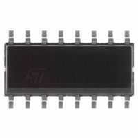
L5991D STMicroelectronics, L5991D Datasheet - Page 9

L5991D
Manufacturer Part Number
L5991D
Description
IC PRIMARY CTRLR W/STANDBY SO16
Manufacturer
STMicroelectronics
Datasheet
1.L5991AD13TR.pdf
(23 pages)
Specifications of L5991D
Mfg Application Notes
25W Off-Line Battery Charger with L5991A AppNote 300W Forward Converter with L5991A AppNote 45W AC-DC Adapter with Standby AppNote 60W Power Supply using the L5991 AppNote 80W Adapter using L6561/L5991A AppNote 90W SMPS for Monitors with Standby AppNote Trick Enhances L5991s Standby Function AppNote L5991-Based Converter, Temp Extra Power AppNote Auxiliary Power Supply Design AppNote Minimize Power Losses AppNote
Pwm Type
Current Mode
Number Of Outputs
1
Frequency - Max
1MHz
Duty Cycle
93%
Voltage - Supply
11 V ~ 20 V
Buck
No
Boost
Yes
Flyback
Yes
Inverting
No
Doubler
No
Divider
No
Cuk
No
Isolated
Yes
Operating Temperature
0°C ~ 105°C
Package / Case
16-SOIC (3.9mm Width)
Frequency-max
1MHz
Duty Cycle (max)
93 %
Output Voltage
5.075 V
Output Current
1500 mA
Mounting Style
SMD/SMT
Switching Frequency
1000 KHz
Operating Supply Voltage
12 V to 20 V
Maximum Operating Temperature
+ 150 C
Fall Time
35 ns
Minimum Operating Temperature
- 40 C
Rise Time
70 ns
Synchronous Pin
Yes
Topology
Boost, Flyback
Number Of Pwm Outputs
1
On/off Pin
No
Adjustable Output
No
Switching Freq
1MHz
Operating Supply Voltage (max)
20V
Operating Temperature Classification
Automotive
Mounting
Surface Mount
Pin Count
16
Package Type
SO
For Use With
497-8226 - BOARD EVAL L5991/STP12NK80Z497-6416 - BOARD EVAL L5991/STP10NK60Z497-5083 - EVAL BOARD 3PH PWR SUPPLY W/ESBT
Lead Free Status / RoHS Status
Lead free / RoHS Compliant
Available stocks
Company
Part Number
Manufacturer
Quantity
Price
Part Number:
L5991D
Manufacturer:
ST
Quantity:
20 000
Company:
Part Number:
L5991D013TR
Manufacturer:
INF
Quantity:
5 383
Part Number:
L5991D013TR
Manufacturer:
ST
Quantity:
20 000
Company:
Part Number:
L5991D013TR-2
Manufacturer:
KODENSHI
Quantity:
2 000
Figure 23. Oscillator and synchronization internal schematic.
The oscillation frequency can be established with
the aid of the diagrams of fig. 14, where R
intended as the parallel of R
operation and R
the following approximate relationships:
which gives the normal operating frequency, and:
which gives the standby frequency, that is the one
the converter will operate at when lightly loaded.
In the above expressions, RA // RB means:
while K
and is related to the duration of the falling-edge of
the sawtooth:
T
ered at pin 1 and defines the upper extreme of the
duty cycle range, D
and calculation) since the output is held low dur-
ing the falling edge.
In case V15 is connected to VREF, however, the
switching frequency will be a half the values taken
d
is also the duration of the sync pulses deliv-
f
R
C
osc
A
T
T
K
f
is defined as:
SB
T
R
T
C
B
d
ST-BY
T
V
RCT
C
90 V
160
REF
30
T
R
T
0.693
A
= R
//
V
4
2
16
0.693 R
x
R
10
15
15
A
B
(see pin 15 for D
STANDBY
9
in standby, or considering
1
1
VREF
GND
R
R
R
A
A
K
A
// R
50
T
A
D1
/OPEN
CLAMP
A
R
R
C
B
B
and R
K
B
T
,
T
K
R3
4 .
T
B
2
X
3 ,
in normal
,
definition
R1
R2
1 ,
T
will be
+
-
from fig. 14 or resulting from (1) and (2).
To prevent the oscillator frequency from switching
back and forth from f
must not exceed 5.5.
If during normal operation the IC is to be synchro-
nized to an external oscillator, R
should be selected for a f
frequency in any condition (typically, 10-20% ),
depending also on the tolerance of the parts.
Pin 3. DC (Duty Cycle Control). By biasing this
pin with a voltage between 1 and 3 V it is possible
to set the maximum duty cycle between 0 and the
upper extreme D
If D
voltage V3 to be applied to pin 3 is:
D
tween V3 and the oscillator ramp (see fig. 24),
thus in case the device is synchronized to an ex-
ternal frequency f
amplitude is reduced), (5) changes into:
A voltage below 1V will inhibit the driver output
stage. This could be used for a not-latched device
disable, for example in case of overvoltage pro-
tection (see application ideas).
If no limitation on the maximum duty cycle is re-
quired (i.e. D
ing. An internal pull-up (see fig. 24) holds the volt-
age above 3V. Should the pin pick up noise (e.g.
max
max
is determined by internal comparison be-
V
3
is the desired maximum duty cycle, the
5 4
MAX
V
3
x
= D
= 5 - 2
ext
(see pin 15).
exp
X
osc
(and therefore the oscillator
), the pin has to be left float-
SYNC
D97IN729A
600 A
(2-Dmax)
to f
osc
R
1
T
SB
lower than the master
D
, the ratio f
C
max
L5991 - L5991A
T
(5)
A
f
ext
, R
D
R
CLK
Q
B
(6)
osc
and C
/ f
9/23
SB
T


