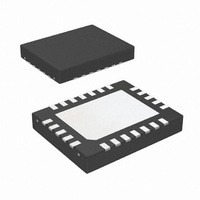
LM5035SQX/NOPB National Semiconductor, LM5035SQX/NOPB Datasheet - Page 5

LM5035SQX/NOPB
Manufacturer Part Number
LM5035SQX/NOPB
Description
IC PWM BUCK BST FLYBCK INV 24LLP
Manufacturer
National Semiconductor
Series
PowerWise®r
Datasheet
1.LM5035SQNOPB.pdf
(28 pages)
Specifications of LM5035SQX/NOPB
Pwm Type
Voltage Mode
Number Of Outputs
1
Frequency - Max
1MHz
Duty Cycle
92%
Voltage - Supply
13 V ~ 105 V
Buck
Yes
Boost
Yes
Flyback
Yes
Inverting
Yes
Doubler
No
Divider
No
Cuk
No
Isolated
Yes
Operating Temperature
-40°C ~ 125°C
Package / Case
24-LLP
Frequency-max
2MHz
For Use With
LM5035EVAL - BOARD EVALUATION LM5035
Lead Free Status / RoHS Status
Lead free / RoHS Compliant
Other names
LM5035SQX
Startup Regulator (VCC pin)
Voltage Reference Regulator (REF pin)
Under-Voltage Lock Out and shutdown (UVLO pin)
Over-Voltage Protection (OVP pin)
Current Sense Input (CS Pin)
Current Limit Restart (RES Pin)
VIN to GND
HS to GND
HB to GND
HB to HS
VCC to GND
CS, RT, DLY to GND
COMP Input Current
Absolute Maximum Ratings
If Military/Aerospace specified devices are required,
please contact the National Semiconductor Sales Office/
Distributors for availability and specifications.
Electrical Characteristics
apply over full Operating Junction Temperature range. V
27.4kΩ, V
Symbol
I
V
VCC(LIM)
V
V
I
V
V
V
VCCUV
I
UVLO
V
I
UVLO
OVP
VIN
VCC
REF
OVP
RES
CS
UVLO
Parameter
VCC voltage
VCC current limit
VCC Under-voltage threshold (VCC
increasing)
VCC decreasing
Startup regulator current
Supply current into VCC from
external source
REF Voltage
REF Voltage Regulation
REF Current Limit
Under-voltage threshold
Hysteresis current
Under-voltage Shutdown Threshold UVLO voltage falling
Under-voltage Standby Enable
Threshold
Over-Voltage threshold
Hysteresis current
Current Limit Threshold
CS delay to output
Leading edge blanking time at CS
CS sink impedance (clocked)
RES Threshold
Charge source current
Discharge sink current
= 3V, V
OVP
= 0V unless otherwise stated. See (Note 2) and (Note 3).
-0.3V to 105V
-1V to 105V
-0.3V to 118V
-0.3V to 18V
-0.3V to 16V
-0.3V to 5.5V
10mA
Specifications with standard typeface are for T
(Note 1)
Conditions
I
V
VIN = VCC, ΔV
setpoint
VCC – PGND
VIN = 90V, UVLO = 0V
Outputs & COMP open, V
Outputs Switching
I
I
REF = 4.5V
UVLO pin sinking
UVLO voltage rising
OVP pin sourcing
CS from zero to 1V. Time for HO and LO
to fall to 90% of VCC. Output load = 0 pF.
Internal FET sink impedance
V
V
VCC
REF
REF
VCC
RES
RES
= 0mA
= 0 to 10mA
= 10mA
= 7V
= 1.5V
= 1V
VIN
= 48V, V
5
VCC
All other inputs to GND
ESD Rating (Note 4)
Storage Temperature Range
Junction Temperature
VIN Voltage
External Voltage Applied to VCC
Operating Junction Temperature
Operating Ratings
Human Body Model
from the regulation
VCC
= 10V externally applied, R
VCC
= 10V,
J
= 25°C, and those with boldface type
1.212
1.212
0.228
4.85
Min
7.3
0.2
5.5
2.4
20
15
19
19
16
8
(Note 1)
RT
= 15.0 kΩ, R
1.25
1.25
0.25
Typ
7.6
0.1
6.2
0.3
0.4
2.5
25
30
25
20
23
23
80
50
32
22
12
4
5
-0.3V to 7V
2kV
-65°C to 150°C
150°C
-40°C to +125°C
1.288
1.288
0.272
Max
5.15
7.9
6.9
2.6
70
50
27
27
60
28
16
13V to 105V
6
www.national.com
DLY
8V to 15V
=
Units
mA
mA
mV
mA
µA
µA
µA
µA
µA
ns
ns
Ω
V
V
V
V
V
V
V
V
V
V


