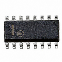
SG3525ADWR2G ON Semiconductor, SG3525ADWR2G Datasheet - Page 4

SG3525ADWR2G
Manufacturer Part Number
SG3525ADWR2G
Description
IC PWM SMPS CONTROLLER 16-SOIC
Manufacturer
ON Semiconductor
Datasheet
1.SG3525ADWR2G.pdf
(10 pages)
Specifications of SG3525ADWR2G
Pwm Type
Voltage Mode
Number Of Outputs
2
Frequency - Max
400kHz
Duty Cycle
49%
Voltage - Supply
8 V ~ 35 V
Buck
No
Boost
No
Flyback
No
Inverting
No
Doubler
No
Divider
No
Cuk
No
Isolated
No
Operating Temperature
0°C ~ 70°C
Package / Case
16-SOIC (0.300", 7.5mm Width)
Frequency-max
400kHz
Number Of Pwm Outputs
2
On/off Pin
Yes
Adjustable Output
No
Switching Freq
400KHz
Operating Supply Voltage (max)
35V
Output Current
400A
Synchronous Pin
Yes
Rise Time
100ns
Fall Time
50ns
Operating Temperature Classification
Commercial
Mounting
Surface Mount
Pin Count
16
Package Type
SOIC W
Topology
Half-Bridge, Push-Pull
Switching Frequency
400 KHz
Duty Cycle (max)
49 %
Maximum Operating Temperature
+ 70 C
Minimum Operating Temperature
0 C
Mounting Style
SMD/SMT
Lead Free Status / RoHS Status
Lead free / RoHS Compliant
Available stocks
Company
Part Number
Manufacturer
Quantity
Price
Part Number:
SG3525ADWR2G
Manufacturer:
ON/安森美
Quantity:
20 000
3. T
4. Since long term stability cannot be measured on each device before shipment, this specification is an engineering estimate of average
5. Tested at f
ELECTRICAL CHARACTERISTICS
REFERENCE SECTION
OSCILLATOR SECTION (Note 5, unless otherwise noted.)
ERROR AMPLIFIER SECTION (V
PWM COMPARATOR SECTION
Reference Output Voltage (T
Line Regulation (+8.0 V
Load Regulation (0 mA
Temperature Stability
Total Output Variation Includes Line and Load Regulation over Temperature
Short Circuit Current (V
Output Noise Voltage (10 Hz
Long Term Stability (T
Initial Accuracy (T
Frequency Stability with Voltage
Frequency Stability with Temperature
Minimum Frequency (R
Maximum Frequency (R
Current Mirror (I
Clock Amplitude
Clock Width (T
Sync Threshold
Sync Input Current (Sync Voltage = +3.5 V)
Input Offset Voltage
Input Bias Current
Input Offset Current
DC Open Loop Gain (R
Low Level Output Voltage
High Level Output Voltage
Common Mode Rejection Ratio (+1.5 V
Power Supply Rejection Ratio (+8.0 V
Minimum Duty Cycle
Maximum Duty Cycle
Input Threshold, Zero Duty Cycle (Note 5)
Input Threshold, Maximum Duty Cycle (Note 5)
Input Bias Current
stability from lot to lot.
(+8.0 V
low
= 0
osc
V
CC
J
= 40 kHz (R
RT
= +25 C)
J
T
+35 V)
= 2.0 mA)
= +25 C)
high
J
ref
T
L
= +125 C) (Note 4)
= +70 C
T
= 150 kW, C
I
= 2.0 kW, C
V
L
= 0 V, T
10 MW)
T
CC
J
= 3.6 kW, C
20 mA)
= +25 C)
f
Characteristics
+35 V)
CM
J
10 kHz, T
= +25 C)
= +5.1 V)
T
T
= 0.2 mF)
= 1.0 nF)
T
V
(V
V
CC
= 0.01 mF, R
CC
CM
J
= +25 C)
= +20 Vdc, T
+35 V)
+5.2 V)
D
= 0 W).
http://onsemi.com
A
= T
SG3525A
low
4
to T
high
[Note 3], unless otherwise noted.)
DV
Symbol
Reg
Reg
CMRR
DC
PSRR
DC
D VCC
Df osc
DV
Df osc
A
f
V
V
V
f
V
I
D T
V
V
ref
max
V
min
I
I
VOL
I
SC
S
IO
IB
OH
IB
ref
OL
IO
max
th
th
min
load
n
ref
line
/DT
5.00
4.95
Min
400
1.7
3.0
0.3
1.2
3.8
0.6
60
60
50
45
−
−
−
−
−
−
−
−
−
−
−
−
−
−
−
−
−
−
5.10
0.05
Typ
2.0
3.5
0.5
2.0
1.0
2.0
1.0
0.2
5.6
0.9
3.3
10
20
20
80
40
20
50
75
75
60
49
2.0
1.0
0.3
−
−
−
−
Max
5.20
5.25
100
200
2.2
1.0
2.8
2.5
1.0
0.5
3.6
1.0
20
50
50
10
10
6.0
2.0
−
−
−
−
−
−
−
−
−
0
−
−
mV/khr
mV
Unit
Vdc
Vdc
kHz
mV
mV
mV
mA
mA
mA
mV
Hz
mA
mA
dB
dB
dB
mA
ms
%
%
%
%
%
V
V
V
V
V
V
rms


