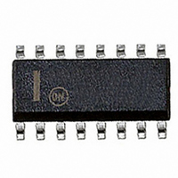
NCP1396BDR2G ON Semiconductor, NCP1396BDR2G Datasheet

NCP1396BDR2G
Specifications of NCP1396BDR2G
NCP1396BDR2GOS
NCP1396BDR2GOSTR
Available stocks
Related parts for NCP1396BDR2G
NCP1396BDR2G Summary of contents
Page 1
NCP1396A, NCP1396B High Performance Resonant Mode Controller featuring High- - Voltage Drivers The NCP1396 A/B offers everything needed to build a reliable and rugged resonant mode power supply. Its unique architecture includes a 500 kHz Voltage Controlled Oscillator whose control ...
Page 2
HV R17 FB OVP U2A U3A Fast Input Fmax C10 C9 C8 R19 R9 R14 R18 R13 R6 Soft- - Timer BO DT Skip start Selection PIN FUNCTION DESCRIPTION Pin No. ...
Page 3
Vdd Vdd Imin Vfb Vfb_off Vref Vref Rt IDT Imax for Vfb = 5 for Vfb < Vfb_min Vdd Imax Vfb = 5 Vdd Vref Itimer Fmax If FAULT Itimer else 0 ...
Page 4
MAXIMUM RATINGS Rating High Voltage bridge pin, pin 14 Floating supply voltage High side output voltage Low side output voltage Allowable output slew rate Power Supply voltage, pin 12 Maximum voltage, all pins (except pin 11 and 10) Thermal Resistance ...
Page 5
ELECTRICAL CHARACTERISTICS (For typical values T = 25C, for min/max values T J Characteristic SUPPLY SECTION Turn- -on threshold level, V going up – A version CC Turn- -on threshold level, V going up – B version CC Minimum operating ...
Page 6
ELECTRICAL CHARACTERISTICS (For typical values T = 25C, for min/max values T J TIMERS Characteristic Timer charge current Timer duration with capacitor and a 1 MΩ resistor Timer recurrence in permanent fault, same values as above Voltage ...
Page 7
TYPICAL CHARACTERISTICS - - A VERSION 13.55 13.5 13.45 13.4 13.35 13.3 13.25 13.2 13.15 13.1 - -40 - - TEMPERATURE (C) Figure 3. V CC(on) 60.2 60.1 60.0 59.9 59.8 59.7 59.6 59.5 ...
Page 8
TYPICAL CHARACTERISTICS - - A VERSION -40 - - TEMPERATURE (C) Figure 9. Source Resistance (ROH) 109 108 107 106 105 104 103 ...
Page 9
TYPICAL CHARACTERISTICS - - A VERSION 1.045 1.040 1.035 1.030 1.025 1.020 - -40 - - TEMPERATURE (C) Figure 15. Brown- -Out Reference (VBO) 26.8 26.6 26.4 26.2 26.0 25.8 25.6 25.4 25.2 25.0 ...
Page 10
TYPICAL CHARACTERISTICS - - B VERSION 10.65 10.60 10.55 10.50 10.45 10.40 10.35 - -40 - - TEMPERATURE (C) Figure 17. V CC(on) 60.1 60.0 59.9 59.8 59.7 59.6 59.5 59.4 59.3 - -40 ...
Page 11
TYPICAL CHARACTERISTICS - - B VERSION -40 - - TEMPERATURE (C) Figure 23. Source Resistance (ROH) 108 107 106 105 104 103 102 ...
Page 12
TYPICAL CHARACTERISTICS - - B VERSION 1.050 1.045 1.040 1.035 1.030 1.025 - -40 - - TEMPERATURE (C) Figure 29. Brown- -Out Reference (VBO) 107 106 105 104 103 102 101 100 99 65 ...
Page 13
The NCP1396 A/B includes all necessary features to help building a rugged and safe switch- - mode power supply featuring an extremely low standby power. The below bullets detail the benefits brought by implementing the NCP1396 controller: Wide frequency ...
Page 14
B is more recommended for industrial / medical applications where auxiliary supply directly powers the chip. 2. The A version does not activate the soft- ...
Page 15
11 100 k 2 8.7 k Figure 32. The OPAMP Arrangement Limits the VCO Modulation Signal between 0.5 and 2.3 V This techniques allows us to detect a fault on the ...
Page 16
RFmin (kΩ) Figure 36. Minimum Switching Frequency Resistor Selection (Fmin = 100 kHz to 500 kHz) 100 ...
Page 17
Vdd Icharge: Fsw min + Fsw max + - - Idis Vref DT RDT Figure 40. Dead- -time Generation http://onsemi.com Clk ...
Page 18
During the discharge time, the clock comparator is high and un- - validates the AND gates: both outputs are low. When the comparator goes back to the low level, during the timing capacitor Ct recharge time, A and B outputs ...
Page 19
Clock Pulses 12.0 8.00 4.00 0 8.00 4. -4. -8.00 56.2 m Brown- -Out Protection The Brown- - Out circuitry (BO) offers a way to protect the ...
Page 20
Figure 45. Simulation Results for 350 / 250 ON / OFF Levels To the contrary, when the internal BO signal is high (Mlower and Mupper pulse), the IBO ...
Page 21
On Figure 46 blocked and does not bother the BO measurement as long as the NTC and the optocoupler are not activated. As soon as the secondary optocoupler senses an OVP condition, or the NTC reacts to a ...
Page 22
VtimerON level (4 V typical), then all pulses are stopped. If the fault input signal is still present, then the controller permanently stays off and the voltage on the timer capacitor does not move (Itimer is on and ...
Page 23
V CC(on) V CC(min 0.6 V A& Timer Figure 50. At power on, output A is first activated and the frequency slowly decreases via the soft- -start capacitor Figure 50 ...
Page 24
... ORDERING INFORMATION Device NCP1396ADR2G NCP1396BDR2G †For information on tape and reel specifications, including part orientation and tape sizes, please refer to our Tape and Reel Packaging Specification Brochure, BRD8011/D. for the direct a connection from source. Thanks to this NCP1396B, simple ON/OFF operation is therefore feasible ...
Page 25
... SEATING C PLANE *For additional information on our Pb- -Free strategy and soldering details, please download the ON Semiconductor Soldering and Mounting Techniques Reference Manual, SOLDERRM/D. ON Semiconductor and are registered trademarks of Semiconductor Components Industries, LLC (SCILLC). SCILLC reserves the right to make changes without further notice to any products herein ...


