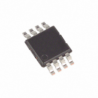
MAX5071AAUA+T Maxim Integrated Products, MAX5071AAUA+T Datasheet - Page 15

MAX5071AAUA+T
Manufacturer Part Number
MAX5071AAUA+T
Description
IC CNTRLR PWM CRNT MD 8-UMAX
Manufacturer
Maxim Integrated Products
Datasheet
1.MAX5070BAUA.pdf
(22 pages)
Specifications of MAX5071AAUA+T
Pwm Type
Current Mode
Number Of Outputs
1
Frequency - Max
1MHz
Duty Cycle
97.5%
Voltage - Supply
10.8 V ~ 25 V
Buck
No
Boost
No
Flyback
Yes
Inverting
No
Doubler
No
Divider
Yes
Cuk
No
Isolated
Yes
Operating Temperature
-40°C ~ 125°C
Package / Case
8-MSOP, Micro8™, 8-uMAX, 8-uSOP,
Frequency-max
1MHz
Duty Cycle (max)
97.5 %
Output Current
2000 mA
Mounting Style
SMD/SMT
Switching Frequency
1000 KHz
Maximum Operating Temperature
+ 125 C
Fall Time
22 ns
Minimum Operating Temperature
- 40 C
Rise Time
15 ns
Synchronous Pin
Yes
Topology
Flyback, Forward, Push-Pull
Lead Free Status / RoHS Status
Lead free / RoHS Compliant
The MAX5071A/MAX5071B/MAX5071C are designed to
be used with either an external error amplifier when
designed into a nonisolated converter or an error ampli-
fier and optocoupler when designed into an isolated
power supply. The COMP input is level-shifted and
connected to the inverting terminal of the PWM com-
parator (CPWM). Connect the COMP pin to the output
of the external error amplifier for nonisolated design.
Pull COMP high externally to at least 5V (or VREF) and
connect the optocoupler transistor as shown in Figures
7 and 8. COMP can be used for soft-start and also as a
shutdown. See the Typical Operating Characteristics to
find the turn-off COMP voltage at different tempera-
tures. If the maximum external COMP voltage is below
4.9V, it may reduce the PWM current-limit threshold
below 1V. Use the following equation to calculate mini-
mum COMP voltage (V
peak primary current (I
where R
The oscillator frequency is adjusted by adding an
external capacitor and resistor at R
in the Typical Application Circuits). R
from R
nected from R
R
through an 8.3mA internal current sink until C
reaches 1.1V, at which time C
through R
sum of the charge and discharge times of C
the charge time as:
The discharge time is then:
The oscillator frequency will then be:
For the MAX5070A/MAX5071A, the converter output
switching frequency (f
frequency (f
MAX5071C, the output switching frequency is 1/2 the
oscillator frequency.
T
High-Performance, Single-Ended, Current-Mode
until its voltage reaches 2.8V. C
T
/C
CS
T
T
V
is a current-sense resistor.
MAX5071A/MAX5071B/MAX5071C
to the 5V reference (VREF) and C
COMP
again. The oscillator’s period will be the
OSC
T
t
D
/C
=
T
t
). For the MAX5070B/MAX5071B/
______________________________________________________________________________________
= (3 x I
C
4 88
to GND. VREF charges C
f
OSC
.
= 0.57 x R
R
SW
COMP
P-P
T
×
) is the same as the oscillator
=
×
R
):
P-P
T
C
t
C
) required for a guaranteed
T
−
x R
1 8 10
+
×
1
T
.
10
T
t
CS
D
x C
×
is allowed to charge
3
T
) + 1.95V
/C
T
T
3
T
then discharges
T
(see R
is connected
Feedback
Oscillator
T
. Calculate
T
T
’s voltage
T
T
through
and C
is con-
T
VREF is a 5V reference output that can source 20mA.
Bypass VREF to GND with a 0.1µF capacitor.
The MAX5070/MAX5071 include a fast current-limit com-
parator to terminate the ON cycle during an overload or a
fault condition. The current-sense resistor (R
ed between the source of the MOSFET and GND, sets
the current limit. The CS input has a voltage trip level
(V
I
the MOSFET. When the voltage produced by this current
(through the current-sense resistor) exceeds the current-
limit comparator threshold, the MOSFET driver (OUT) will
turn the switch off within 60ns. In most cases, a small RC
filter is required to filter out the leading-edge spike on the
sense waveform. Set the time constant of the RC filter at
50ns. Use a current transformer to limit the losses in the
current-sense resistor and achieve higher efficiency
especially at low input-voltage operation.
SYNC is a bidirectional input/output that outputs a syn-
chronizing pulse and accepts a synchronizing pulse
from other MAX5071A/MAX5071Bs (see Figures 7 and
9). As an output, SYNC is an open-drain p-channel
MOSFET driven from the internal oscillator and requires
an external pulldown resistor (R
500Ω and 5kΩ. As an input, SYNC accepts the output
pulses from other MAX5071A/MAX5071Bs.
Synchronize multiple MAX5071A/MAX5071Bs by con-
necting their SYNC pins together. All devices connected
together will synchronize to the one operating at the
highest frequency. The rising edge of SYNC will precede
the rising edge of OUT by approximately the discharge
time (t
pulse width of the SYNC output is equal to the time
required to discharge the stray capacitance at SYNC
through R
R
P-P
T
CS
/C
Synchronization (MAX5071A/MAX5071B)
is the peak current in the primary that flows through
) of 1V. Use the following equation to calculate R
T
D
such that the minimum discharge time t
) of the oscillator (see the Oscillator section). The
SYNC
PWM Controllers
plus the C
R
CS
=
T
I
V
P P
discharge time t
CS
−
Reference Output
SYNC
Current Limit
) from between
CS
D
), connect-
D
is 200ns.
. Adjust
SYNC
CS
15
:


