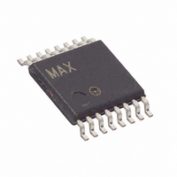
MAX15004BAUE+ Maxim Integrated Products, MAX15004BAUE+ Datasheet - Page 17

MAX15004BAUE+
Manufacturer Part Number
MAX15004BAUE+
Description
IC PWR SUPPLY CNTRLR 16-TSSOP
Manufacturer
Maxim Integrated Products
Datasheet
1.MAX15005BAUE.pdf
(27 pages)
Specifications of MAX15004BAUE+
Pwm Type
Current Mode
Number Of Outputs
1
Frequency - Max
1MHz
Duty Cycle
50%
Voltage - Supply
4.5 V ~ 40 V
Buck
No
Boost
Yes
Flyback
Yes
Inverting
No
Doubler
No
Divider
Yes
Cuk
No
Isolated
Yes
Operating Temperature
-40°C ~ 125°C
Package / Case
16-TSSOP
Frequency-max
1MHz
Duty Cycle (max)
50 %
Output Voltage
1.23 V to 100 V
Output Current
1000 mA
Mounting Style
SMD/SMT
Switching Frequency
15 KHz to 500 KHz
Operating Supply Voltage
4.5 V to 40 V
Maximum Operating Temperature
+ 125 C
Minimum Operating Temperature
- 40 C
Synchronous Pin
Yes
Topology
Boost, Flyback, Forward
Lead Free Status / RoHS Status
Lead free / RoHS Compliant
I
to the capacitor discharge, and ΔV
due to the ESR of the capacitor. D
duty cycle at the minimum input voltage. Use a combina-
tion of low-ESR ceramic and high-value, low-cost alu-
minum capacitors for lower output ripple and noise.
The MAX15004A/MAX15005A devices are available in
a thermally enhanced package and can dissipate up to
1.7W at +70°C ambient temperature. The total power
dissipation in the package must be limited so that the
junction temperature does not exceed its absolute max-
imum rating of +150°C at maximum ambient tempera-
ture; however, Maxim recommends operating the
junction at about +125°C for better reliability.
The average supply current (I
the switch driver is:
where Q
able from MOSFET datasheet.
The supply current in the MAX15004A/B/MAX15005A/B
is dependent on the switching frequency. See the
Typical Operating Characteristics to find the supply
current I
a given operating frequency. The total power dissipa-
tion (P
and the current required to drive the switch (I
GATE
The MAX15004A/B/MAX15005A/B drive a wide variety of
n-channel power MOSFETs. Since V
output peak gate-drive voltage to no more than 11V, a
12V (max) gate voltage-rated MOSFET can be used with-
out an additional clamp. Best performance, especially at
low-input voltages (5V
n-channel MOSFETs that specify on-resistance with a
gate-source voltage (V
the MOSFET, key parameters can include:
1) Total gate charge (Q
O
Flyback/Boost/SEPIC Power-Supply Controllers
is the load current, ΔV
) is calculated using following equation.
T
) in the device due to supply current (I
P
g
SUPPLY
T
Calculating Power Loss in Boost Converter
is total gate charge at 7.4V, a number avail-
=
V
INMAX
I
MOSFET Selection in Boost Converter
DRIVE GATE
of the MAX15004A/B/MAX15005A/B at
ESR
C
______________________________________________________________________________________
OUT
−
×
=
IN
GS
(
I
), is achieved with low-threshold
g
=
Δ
Q
SUPPLY
) of 2.5V or less. When selecting
).
V
I
Δ
is the portion of the ripple due
I
O
ESR
O
V
=
Q
×
Q
DRIVE-GATE
D
×
g
+
MAX
f
OUT
I
ESR
×
DRIVE GATE
MAX
f
OUT
CC
is the contribution
is the maximum
−
limits the OUT
) required by
4.5V to 40V Input Automotive
)
SUPPLY
DRIVE-
)
2) Reverse-transfer capacitance or charge (C
3) On-resistance (R
4) Maximum drain-to-source voltage (V
5) Maximum gate frequencies threshold voltage
At high switching, dynamic characteristics (parameters 1
and 2 of the above list) that predict switching losses
have more impact on efficiency than R
dicts DC losses. Q
ed with charging the gate. The V
MOSFET must be greater than the maximum output volt-
age setting plus a diode drop. The 10V additional margin
is recommended for spikes at the MOSFET drain due to
the inductance in the rectifier diode and output capacitor
path. In addition, Q
drive the gate at the selected operating frequency when
the internal LDO is driving the MOSFET.
The MAX15004A/B/MAX15005A/B use an internal ramp
generator for slope compensation to stabilize the current
loop when operating at duty cycles above 50%. It is
advisable to add some slope compensation even at lower
than 50% duty cycle to improve the noise immunity. The
slope compensations should be optimized because too
much slope compensation can turn the converter into the
voltage-mode control. The amount of slope compensation
required depends on the downslope of the inductor cur-
rent when the main switch is off. The inductor downslope
depends on the input to output voltage differential of the
boost converter, inductor value, and the switching fre-
quency. Theoretically, the compensation slope should be
equal to 50% of the inductor downslope; however, a little
higher than 50% slope is advised.
Use the following equation to calculate the required
compensating slope (mc) for the boost converter:
The internal ramp signal resets at the beginning of
each cycle and slews at the rate programmed by the
external capacitor connected to SLOPE. Adjust the
MAX15004A/B/MAX15005A/B slew rate up to 110mV/μs
using the following equation:
where C
farads.
(V
TH(MAX)
mc
Slope Compensation in Boost Configuration
SLOPE
=
).
(
V
OUT
is the external capacitor at SLOPE in
C
g
SLOPE
g
DS(ON)
includes all capacitances associat-
helps predict the current needed to
−
V
IN
2
=
)
L
).
×
mc mV s
2 5 10
R
.
S
(
×
×
DS(MAX)
10
μ
−
−
9
DS(ON)
3
)
DS(MAX)
(
mV s
of the selected
μ
, which pre-
RSS
)
).
).
17


