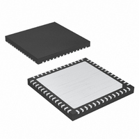
MAX5043ETN+T Maxim Integrated Products, MAX5043ETN+T Datasheet - Page 13

MAX5043ETN+T
Manufacturer Part Number
MAX5043ETN+T
Description
IC PWR W/MOSFET HS 56-TQFN
Manufacturer
Maxim Integrated Products
Datasheet
1.MAX5042ATN.pdf
(22 pages)
Specifications of MAX5043ETN+T
Package / Case
56-TQFN
Voltage - Supply
20 V ~ 76 V
Frequency-max
500kHz
Operating Temperature
-40°C ~ 85°C
Number Of Outputs
1
Duty Cycle
47%
Pwm Type
Voltage/Current Mode
Buck
No
Boost
No
Flyback
Yes
Inverting
No
Doubler
No
Divider
No
Cuk
No
Isolated
Yes
Lead Free Status / RoHS Status
Lead free / RoHS Compliant
Set the switching frequency with a resistor and a
capacitor at RCOSC. Switching at 250kHz ensures
switching losses are minimal and external power pas-
sives are small enough for a compact circuit.
The MAX5042/MAX5043 incorporate an advanced set of
protection features that make them uniquely suitable
when high reliability and comprehensive fault protection
are required, as in telecommunication equipment power-
supply applications. The MAX5042/MAX5043 15V linear
regulator output powers the 9V and 5V regulators used to
drive the gates and internal circuitry. A tertiary winding
connects to REG15 through a rectifier to power the
device after startup and reduces power dissipation in the
MAX5042/MAX5043 package. When REG15 is externally
powered, the internal 15V regulator is disabled.
Figures 3 and 4 show the block diagrams of the MAX5042
and MAX5043, respectively. The power-OK signals from
the hot-swap section, regulators, thermal shutdown, and
UVLO combine to generate the internal shutdown signal
SHDN. When asserted, SHDN disables the comparators
and oscillator. Deasserting SHDN releases the compara-
tors and oscillators. The falling edge of SHDN is delayed
allowing the internal signals to settle before the PWM puls-
es appear. During the time between the falling edge of
SHDN and its delayed signal, the 10Ω internal MOSFET
(QB) from XFRMRH to PWMPNEG turns on, charging the
BST capacitor. After startup, this MOSFET also turns on
for approximately 300ns at each half period to help
charge the BST capacitor.
Figure 2. Simplified Diagram of a MAX5043-Based Isolated
Power Supply
+V
POSINPWM
PWMNEG
INTEGRATED
CIRCUIT
PWM
WITH
MAX5043
FETs
QH
QL
Power MOSFETs and Hot-Swap Controller
______________________________________________________________________________________
Two-Switch Power ICs with Integrated
C
IN
T1
BULK STORAGE CAPACITOR
L
C
OUT
V
OUT
The two-switch forward-converter topology offers out-
standing robustness against faults and transformer satu-
ration while affording efficient use of the integrated
75mΩ power MOSFETs. Voltage-mode control with feed-
forward compensation allows the rejection of input sup-
ply disturbances within a single cycle similar to that of
current-mode controlled topologies. This control method
offers some significant benefits when compared with
current-mode control. These benefits include:
• No minimum duty-cycle requirement due to current-
• Clean modulator ramp and higher amplitude for
• Stable bias point of the optocoupler LED and photo-
• Predictable loop dynamics simplifying the design of
The two-switch power topology recovers energy stored
in both the magnetizing and parasitic leakage induc-
tances of the transformer. Figure 7 shows the schemat-
ic diagram of a 48V input and 5V, 8A output isolated
power supply built with the MAX5042.
The MAX5042/MAX5043 also support current-mode con-
trol. Current-mode control has advantages such as a sin-
gle-pole power circuit and a small-signal transfer
function that simplify the design of power supplies with
widely varying output capacitors.
The MAX5042 has two UVLO functions. Both the hot-
swap section and the PWM section contain their own
undervoltage lockout comparators (HSEN and UVLO,
respectively). The MAX5043 lacks the hot-swapping
function, but retains the PWM UVLO and the deglitched
undervoltage lockout/power-on reset. In both cases,
internal resistors set a default input-voltage enable
threshold of 31V (typ).
The PWM default input voltage threshold value can be
adjusted by using an external divider in parallel with the
internal divider. The tolerances of the external divider
resistors dominate the precision of the UVLO trip point if
their values are smaller than those of the internal divider.
Override the default threshold by using:
R
signal filtering or blanking.
increased stability.
transistor for maximized control-loop bandwidth (in
current-mode applications, the optocoupler bias
point is output-load dependent).
the control loop.
He
=
V
REF
×
R
Hi
R
Le
(
R
×
Li
R
+
Li
R
×
Le
Undervoltage Lockout
R
)
Hi
-
R
×
Le
(
V
×
IN
Power Topology
R
-
Li
V
REF
×
(
V
IN
)
-
V
REF
)
13


