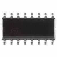
E-SG3525AP STMicroelectronics, E-SG3525AP Datasheet

E-SG3525AP
Specifications of E-SG3525AP
Available stocks
Related parts for E-SG3525AP
E-SG3525AP Summary of contents
Page 1
... A sync input to the oscillator al- lows multiple units to be slaved or a single unit to be synchronized to an external system clock. A single resistor between the C and the discharge terminals ...
Page 2
... Symbol R Thermal Resistance Junction-pins th j-pins R Thermal Resistance Junction-ambient th j-amb R Thermal Resistance Junction-alumina (*) th j-alumina * Thermal resistance junction-alumina with the device soldered on the middle of an alumina supporting substrate measuring 0.65 mm thickness with infinite heatsink. BLOCK DIAGRAM 2/12 Parameter Terminal = 70 C amb SG3525A Parameter ...
Page 3
... ELECTRICAL CHARACTERISTICS ( and over operating temperature, unless otherwise specified) Symbol Parameter REFERENCE SECTION V Output Voltage REF V Line Regulation REF V Load Regulation REF Temp. Stability REF * Total Output Variation Short Circuit Current * Output Noise Voltage V * Long Term Stability REF OSCILLATOR SECTION * * *, ...
Page 4
... Output Low Level Output High Level Under-Voltage Lockout I Collector Leakage Rise Time Fall Time f TOTAL STANDBY CURRENT I Supply Current s * These parameters, although guaranteed over the recommended operating conditions, are not 100 % tested in production. Tested KHz ( osc (0 transconductance (g ) relates to DC open-loop voltage gain (G M from pin 9 to ground ...
Page 5
... TEST CIRCUIT SG2525A-SG3525A 5/12 ...
Page 6
... Sink/Source Load Current (peak) Reference Load Current Oscillator Frequency Range Oscillator Timing Resistor Oscillator Timing Capacitor Dead Time Resistor Range ( ) Range over which the device is functional and parameter limits are guaranteed. Figure 1 : Oscillator Charge Time vs. R and Figure 3 : Output Saturation Characteristics. ...
Page 7
... Since both the compensation and soft-start termi- nals (Pins 9 and 8) have current source pull-ups, either can readily accept a pull-down signal which only has to sink a maximum of 100 A to turn off the outputs. This is subject to the added requirement of discharging whatever external capacitance may be attached to these pins ...
Page 8
... SG2525A-SG3525A Figure 6 : Oscillator Schematic. Figure 7 : Output Circuit (1/2 circuit shown). 8/12 ...
Page 9
... In conventional push-pull bipolar designs, forward base drive is controlled times for the power devices are achieved with speed-up capacitors C and Figure 11. Low power transformers can be driven directly. Automatic reset occurs during dead time, when both ends of the primary winding are switched to ground Rapid turn-off 3 . 9/12 ...
Page 10
... SG2525A-SG3525A mm DIM. MIN. TYP. MAX. MIN. a1 0.51 0.020 B 0.77 1.65 0.030 b 0 8.5 e 2.54 e3 17.78 F 7.1 I 5.1 L 3.3 Z 1.27 10/12 inch MECHANICAL DATA TYP. MAX. 0.065 0.020 0.010 0.787 0.335 0.100 0.700 0.280 0.201 0.130 0.050 OUTLINE AND DIP16 ...
Page 11
... G 4.6 5.3 0.181 L 0.4 1.27 0.016 M 0.62 8˚(max.) S (1) D and F do not include mold flash or protrusions. Mold flash or potrusions shall not exceed 0.15mm (.006inch). inch TYP. MAX. MECHANICAL DATA 0.069 0.009 0.063 0.018 0.010 0.020 0.394 0.244 0.050 0.350 ...
Page 12
... STMicroelectronics. The ST logo is a registered trademark of STMicroelectronics © 2000 STMicroelectronics – Printed in Italy – All Rights Reserved Australia - Brazil - China - Finland - France - Germany - Hong Kong - India - Italy - Japan - Malaysia - Malta - Morocco - Singapore - Spain - Sweden - Switzerland - United Kingdom - U.S.A. 12/12 STMicroelectronics GROUP OF COMPANIES ...


