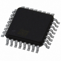
L5994A STMicroelectronics, L5994A Datasheet - Page 10

L5994A
Manufacturer Part Number
L5994A
Description
IC CTRLR PS ADJ TRPL-OUT 32-TQFP
Manufacturer
STMicroelectronics
Datasheet
1.L5994.pdf
(26 pages)
Specifications of L5994A
Pwm Type
Current Mode
Number Of Outputs
3
Frequency - Max
345kHz
Duty Cycle
96%
Voltage - Supply
4.75 V ~ 25 V
Buck
Yes
Boost
No
Flyback
Yes
Inverting
No
Doubler
No
Divider
No
Cuk
No
Isolated
No
Operating Temperature
-40°C ~ 140°C
Package / Case
32-TQFP, 32-VQFP
Frequency-max
345kHz
Lead Free Status / RoHS Status
Lead free / RoHS Compliant
Other names
497-5340
L5994A
L5994A
Available stocks
Company
Part Number
Manufacturer
Quantity
Price
L5994 - L5994A
Although the Schottky might appear to be redundant, it is not in a system where a very high efficiency is re-
quired. In fact, its lower threshold prevents the lossy body-diode of the synchronous rectifier MOSFET from turn-
ing on during the above mentioned dead-time. Both conduction and reverse recovery losses are cut down and
efficiency can improve of 1-2% in some cases. Besides a small diode is sufficient since it conducts for a very
short time.
See the "Power Management" section to see how both synchronous rectifiers are used to ensure zero voltage
output in stand-by conditions or in case of overvoltage.
Pulse-skipping operation
To achieve high efficiency at light load current as well, under this condition the regulators change their operation
(unless this feature is disabled): they abandon PWM and enter the so-called pulse-skipping mode, in which a
single switching cycle takes place every many oscillator periods.
The "light load condition" is detected when the voltage across the external sense resistor (V
exceed the pulse skipping threshold (13mV typ.) while the high-side MOSFET is conducting. When the reset
signal of the output latch comes from the error summing comparator while V
nored and the actual reset is driven as soon as V
extra energy that maintains the output voltage above its nominal value for a while. The oscillator pulses now set
the output latch only when the feedback signal indicates that the output voltage has fallen below its nominal
value. In this way, most of oscillator pulses are skipped and the resulting switching frequency is much lower, as
expressed by the following relationship:
where K = 3.2×10
account for power dissipation at low output power, are considerably reduced.
The section 1 can work with the input voltage very close to the output one (i.e. the output voltage is 5V), where
the current waveform may be so flat to prevent pulse-skipping from being activated. To avoid this, the pulse-
skipping threshold (of section 1 only) is roughly halved at low input voltages (V
in the above formula the constant K becomes 12.8×10
When in pulse-skipping, the output voltage is some ten mV higher than in PWM mode, just because of its mode
of operation. If this "load regulation" effect is undesirable for any reason, the pulse skipping feature can be dis-
abled (see "Power Management" section) to the detriment of efficiency at light load.
MOSFET's Drivers
To get the gate-drive voltage for the high-side N-channel MOSFET a bootstrap technique is employed. A ca-
pacitor is alternately charged through a diode from the 5V PREG5 line when the high-side MOSFET is OFF and
then connected to its gate-source leads by the internal floating driver to turn the MOSFET on. The PREG5 line
is used to drive the synchronous rectifier as well, and therefore the use of low-threshold MOSFET's (the so-
called "logic-level" devices) is highly recommended.
The drivers are of "dynamic" type, which means they do not give origin to current consumption when they are
in static conditions (ON or OFF), but only during transitions. This feature is aimed at minimizing the power con-
sumption of the device even during stand-by when both low-side MOSFET's are ON.
Adaptative anti shoot-through protection is implemented to prevent cross-conduction: the low side mosfet turn
on is disbled until the HSRC pin is above 2V and, in the same way, the high side mosfet turn on is disabled until
the RGATE pin is above 0.3V. During the time in which both mosfets are in off state, the recirculation of the
current is insured by the schottky diode. The resulting dead time depends on the mosfets used and on the cur-
rent flowing in the inductor; in this way many kinds of mosfets may be used and cross conduction is avoided.
10/26
3
and f
PS
is in Hz. As a result, the losses due to switching and to gate-drive, which mostly
f
PS
=
K
R
--------------------- - I
2
S ENSE
L
RSENSE
OUT
3
.
reaches the pulse skipping threshold. This gives some
V
OUT
1
–
V
-------------- -
V
OUT
IN
RSENSE
IN
< 6.8V). Under this condition,
is below this value, it is ig-
RSENSE
) does not


