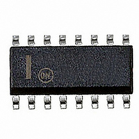
CS51023AEDR16 ON Semiconductor, CS51023AEDR16 Datasheet - Page 5

CS51023AEDR16
Manufacturer Part Number
CS51023AEDR16
Description
IC CTRLR PWM ENHANCE SYNC 16SOIC
Manufacturer
ON Semiconductor
Datasheet
1.CS51021AEDR16G.pdf
(11 pages)
Specifications of CS51023AEDR16
Pwm Type
Current Mode
Number Of Outputs
1
Frequency - Max
1MHz
Duty Cycle
83%
Voltage - Supply
8.2 V ~ 20 V
Buck
Yes
Boost
No
Flyback
No
Inverting
Yes
Doubler
No
Divider
No
Cuk
No
Isolated
No
Operating Temperature
-40°C ~ 85°C
Package / Case
16-SOIC (3.9mm Width)
Frequency-max
1MHz
Lead Free Status / RoHS Status
Contains lead / RoHS non-compliant
Other names
CS51023AEDR16OSTR
Available stocks
Company
Part Number
Manufacturer
Quantity
Price
Company:
Part Number:
CS51023AEDR16
Manufacturer:
TOSHIBA
Quantity:
2 638
ELECTRICAL CHARACTERISTICS
3.0 V < V
PACKAGE PIN DESCRIPTION
Current Sense
OV & UV Voltage Monitors
SOFT START (SS)
4. Guaranteed by design, not 100% tested in production.
16 Lead SO Narrow
OFFSET Voltage
Blanking Time
Blanking Disable Voltage
Second Current Threshold Gain
I
Minimum On Time
Gain
OV Monitor Threshold
OV Hysteresis Current
UV Monitor Threshold
UV Monitor Hysteresis
Charge Current
Discharge Current
Charge Voltage, V
Discharge Voltage, V
SENSE
PIN #
10
12
13
14
15
16
11
1
2
3
3
4
5
6
7
8
9
Input Resistance
C
Characteristic
< 20 V, 8.2 V < V
SLEEP (CS51022A/4A)
SYNC (CS51021A/3A)
PIN SYMBOL
SS
SLOPE
I
COMP
PGND
GATE
LGND
SENSE
R
V
I
V
V
OV
UV
SET
SS
V
T
REF
SS
CC
FB
C
C
T
CC
< 20 V, R
CS51021A, CS51022A, CS51023A, CS51024A
External power switch driver with 1.0 A peak capability.
Current sense amplifier input.
Bi−directional synchronization. Locks to the highest frequency.
Active high chip disable. In sleep mode, V
Additional slope to the current sense signal. Internal current source charges the external capacitor.
Undervoltage protection monitor.
Overvoltage protection monitor.
Timing resistor R
Voltage at this pin sets pulse−by−pulse overcurrent threshold, and second threshold (1.33 times
higher) with Soft Start retrigger (hiccup mode).
Feedback voltage input. Connected to the error amplifier inverting input.
Error amplifier output. Frequency compensation network is usually connected between COMP and
V
Charging external capacitor restricts error amplifier output voltage during the start or fault
conditions (hiccup).
Logic ground.
5.0 V reference voltage output.
Logic supply voltage.
Output power stage ground connection.
Output power stage supply voltage.
(Note 4)
Adjust V
GATE High to Low
(Note 4)
SS = 2.0 V
SS = 2.0 V
FB
T
(Unless otherwise stated, specifications apply for −40°C < T
pins.
= 12 kW, C
FB
Test Conditions
T
T
= 390 pF)
and capacitor C
http://onsemi.com
−
−
−
−
−
−
−
−
−
5
T
determine oscillator frequency and maximum duty cycle, D
REF
FUNCTION
and GATE are turned off.
0.09
1.21
0.78
1.38
0.25
Min
−10
−70
250
1.8
2.4
4.4
30
25
−
−
A
< 85°C, −40°C < T
−12.5
1000
0.10
1.33
0.80
1.45
0.27
Typ
−55
2.0
5.0
2.5
4.7
55
70
75
1.45
0.82
1.52
0.30
Max
0.11
160
−15
100
−40
110
2.2
2.6
5.0
J
−
−
< 150°C,
Unit
V/V
V/V
mV
MAX.
kW
mA
mA
mA
ns
ns
V
V
V
V
V
V


