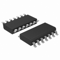
MC33060ADR2G ON Semiconductor, MC33060ADR2G Datasheet - Page 2

MC33060ADR2G
Manufacturer Part Number
MC33060ADR2G
Description
IC CTRLR PWM FIXED FREQ 14SOIC
Manufacturer
ON Semiconductor
Datasheet
1.MC34060APG.pdf
(16 pages)
Specifications of MC33060ADR2G
Pwm Type
Voltage Mode
Number Of Outputs
1
Frequency - Max
200kHz
Duty Cycle
100%
Voltage - Supply
7 V ~ 40 V
Buck
Yes
Boost
Yes
Flyback
Yes
Inverting
Yes
Doubler
No
Divider
No
Cuk
No
Isolated
Yes
Operating Temperature
-40°C ~ 85°C
Package / Case
14-SOIC (3.9mm Width), 14-SOL
Frequency-max
200kHz
Topology
Flyback
Output Voltage
30 V
Output Current
200 mA
Switching Frequency
200 KHz
Duty Cycle (max)
96 %
Operating Supply Voltage
15 V
Maximum Operating Temperature
+ 85 C
Minimum Operating Temperature
- 40 C
Fall Time
40 ns
Mounting Style
SMD/SMT
Rise Time
100 ns
Synchronous Pin
No
Lead Free Status / RoHS Status
Lead free / RoHS Compliant
Other names
MC33060ADR2GOS
Available stocks
Company
Part Number
Manufacturer
Quantity
Price
Company:
Part Number:
MC33060ADR2G
Manufacturer:
ON Semiconductor
Quantity:
500
Part Number:
MC33060ADR2G
Manufacturer:
ON/安森美
Quantity:
20 000
Stresses exceeding Maximum Ratings may damage the device. Maximum Ratings are stress ratings only. Functional operation above the
Recommended Operating Conditions is not implied. Extended exposure to stresses above the Recommended Operating Conditions may affect
device reliability.
1. This device series contains ESD protection and exceeds the following tests:
2. This device contains Latch−Up protection and exceeds ± 100 mA per JEDEC Standard JESD78.
3. Maximum thermal limits must be observed.
MAXIMUM RATINGS
THERMAL CHARACTERISTICS
RECOMMENDED OPERATING CONDITIONS
Power Supply Voltage
Collector Output Voltage
Collector Output Current (Note 3)
Amplifier Input Voltage Range
Power Dissipation @ T
Operating Junction Temperature
Storage Temperature Range
Operating Ambient Temperature Range
ESD Capability
Thermal Resistance, Junction−to−Ambient
Derating Ambient Temperature
Power Supply Voltage
Collector Output Voltage
Collector Output Current
Amplifier Input Voltage
Current Into Feedback Terminal
Reference Output Current
Timing Resistor
Timing Capacitor
Oscillator Frequency
PWM Input Voltage (Pins 3 and 4)
Pins 1– 14: Human Body Model 2000 V per JEDEC Standard JESD22−A114E.
Pins 1– 8:
Machine Model Method 200 V per JEDEC Standard JESD22−A115−A.
A
(Full operating ambient temperature range applies, unless otherwise noted.)
≤ 45°C
Condition/Value
Characteristics
Rating
http://onsemi.com
Human Body Model
For MC34060A
For MC33060A
Machine Model
2
Symbol
Symbol
Symbol
R
V
V
T
f
V
V
P
V
V
I
R
C
T
T
T
osc
I
I
I
ref
stg
qJA
−
CC
CC
fb
C
C
C
in
D
A
A
C
in
J
T
T
0.00047
−0.3
−0.3
Package
Min
P Suffix
7.0
1.8
1.0
−
−
−
−
80
45
−55 to +125
−0.3 to +42
−40 to +85
0 to +70
Value
0.001
1000
Typ
500
125
200
2.0
42
42
15
30
47
25
−
−
−
−
−
Package
D Suffix
120
45
V
Max
CC
200
500
200
0.3
5.3
40
40
10
10
−2
°C/W
Unit
Unit
Unit
mW
kHz
mA
mA
mA
mA
kW
°C
°C
°C
kV
°C
mF
V
V
V
V
V
V
V
V


