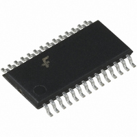
FAN5094MTCX Fairchild Semiconductor, FAN5094MTCX Datasheet - Page 20

FAN5094MTCX
Manufacturer Part Number
FAN5094MTCX
Description
IC CTRLR DC/DC SYNC BUCK 28TSSOP
Manufacturer
Fairchild Semiconductor
Datasheet
1.FAN5094MTCX.pdf
(22 pages)
Specifications of FAN5094MTCX
Applications
Controller, Intel Pentium® IV
Voltage - Input
12V
Number Of Outputs
1
Voltage - Output
1.1 ~ 1.85 V
Operating Temperature
0°C ~ 70°C
Mounting Type
Surface Mount
Package / Case
28-TSSOP
Output Voltage
1.85 V
Output Current
60 A
Mounting Style
SMD/SMT
Maximum Operating Temperature
+ 70 C
Minimum Operating Temperature
0 C
Lead Free Status / RoHS Status
Lead free / RoHS Compliant
Other names
FAN5094MTCXTR
FAN5094MTCX_NL
FAN5094MTCX_NLTR
FAN5094MTCX_NLTR
FAN5094MTCX_NL
FAN5094MTCX_NLTR
FAN5094MTCX_NLTR
FAN5094
PCB Layout Guidelines
• Placement of the MOSFETs relative to the FAN5094 is
• In general, all of the noisy switching lines should be kept
• Place the 0.1µF decoupling capacitors as close to the
• Each power and ground pin should have its own via to the
• Place the MOSFETs, inductor, and Schottky of a given
• Place the output bulk capacitors as close to the CPU as
• A PC Board Layout Checklist is available from Fairchild
20
critical. Place the MOSFETs such that the trace length of
the HIDRV and LODRV pins of the FAN5094 to the FET
gates is minimized. A long lead length on these pins will
cause high amounts of ringing due to the inductance of the
trace and the gate capacitance of the FET. This noise
radiates throughout the board, and, because it is switching
at such a high voltage and frequency, it is very difficult to
suppress.
away from the quiet analog section of the FAN5094. That
is, traces that connect to pins 9-20 (LDRV, HDRV, GND
and BOOT) should be kept far away from the traces that
connect to pins 1 through 8, and pins 21-28.
FAN5094 pins as possible. Extra lead length on these
reduces their ability to suppress noise.
appropriate plane. This helps provide isolation between
pins.
phase as close together as possible for the same reasons as
in the first bullet above. Place the input bulk capacitors as
close to the drains of the high side MOSFETs as possible.
In addition, placement of a 0.1 F decoupling cap right on
the drain of each high side MOSFET helps to suppress
some of the high frequency switching noise on the input
of the DC-DC converter.
possible to optimize their ability to supply instantaneous
current to the load in the event of a current transient.
Additional space between the output capacitors and the
CPU will allow the parasitic resistance of the board traces
to degrade the DC-DC converter’s performance under
severe load transient conditions, causing higher voltage
deviation. For more detailed information regarding
capacitor placement, refer to Application Bulletin AB-5.
Applications. Ask for Application Bulletin AB-11.
PC Motherboard Sample Layout and Gerber File
A reference design for motherboard implementation of the
FAN5094 along with the PCAD layout Gerber file and silk
screen can be obtained through your local Fairchild represen-
tative.
FAN5094 Evaluation Board
Fairchild provides an evaluation board to verify the system
level performance of the FAN5094. It serves as a guide to
performance expectations when using the supplied external
components and PCB layout. Please contact your local
Fairchild representative for an evaluation board.
Additional Information
For additional information contact your local Fairchild
representative.
PRODUCT SPECIFICATION
REV. 1.0.2 5/13/02


