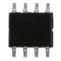
SC2596SETRT Semtech, SC2596SETRT Datasheet - Page 10

SC2596SETRT
Manufacturer Part Number
SC2596SETRT
Description
IC INTEGRTD DDR TERM REG 8-SOIC
Manufacturer
Semtech
Datasheet
1.SC2596SETRT.pdf
(14 pages)
Specifications of SC2596SETRT
Applications
Converter, DDR
Number Of Outputs
1
Operating Temperature
-40°C ~ 105°C
Mounting Type
Surface Mount
Package / Case
8-SOIC
Lead Free Status / RoHS Status
Lead free / RoHS Compliant
Voltage - Output
-
Voltage - Input
-
Other names
SC2596SETR
Available stocks
Company
Part Number
Manufacturer
Quantity
Price
Company:
Part Number:
SC2596SETRT
Manufacturer:
SEMTECH
Quantity:
15 000
Part Number:
SC2596SETRT
Manufacturer:
SEMTECH/美国升特
Quantity:
20 000
Application_2: Lower Power Loss Configuration for
SSTL-2
If power loss is a major concern, separating the PVCC
form AVCC and VDDQ will be a good choice (Figure 2).
The PVCC can operate at lower voltage (1.8V to 2.5V) if
2.5V voltage is applied on AVCC and the VDDQ, the source
current is lower due to the lower operating voltage ap-
plied on the PVCC.
Application_3: Low Power Loss Configuration for
SSTL-18(DDR-II)
If power loss is a major concern, setting the PVCC to be
2.5V will be a good choice (Figure 3). The PVCC can op-
erate at lower voltage. if 2.5V voltage is applied on AVCC
and PVCC, the source current is lower due to the lower
operating voltage applied on the PVCC.
© 2009 Semtech Corp.
POWER MANAGEMENT
Application Information (Cont.)
VREF/0.9V
VREF/1.25V
Notes:
(a) The preferred configuration for DDR-I applications is to tie AVCC and PVCC to VDDQ, which is typically 2.5V.
(b) If AVCC and PVCC rails are tied together, then the VDDQ cannot lead the AVCC and PVCC.
EN
EN/2.5V
Figure 3: Lower power loss for SSTL-18(DDR-II).
Figure 2: Lower power loss for SSTL-2(DDR-I).
0
0
Csense
Csense
100nF
100nF
Csense
Csense
100nF
100nF
1M
1M
1M
1M
100nF
100nF
CREF
CREF
100nF
100nF
CREF
CREF
1
2
3
4
1
2
3
4
GND
EN
VSENSE
VREF
GND
EN
VSENSE
VREF
SC2596
SC2596
SC2596
SC2596
VDDQ
PVCC
AVCC
VDDQ
PVCC
AVCC
VTT
VTT
8
7
6
5
8
7
6
5
CIN1
CIN1
VDDQ/AVCC=2.5V
CIN1
CIN1
VDDQ=1.8V
AVCC/PVCC=2.5V
1uF
1uF
1uF
1uF
CIN2
CIN2
CIN2
CIN2
PVCC=2.5V
100uF
100uF
100uF
100uF
COUT
COUT
COUT
COUT
220uF
220uF
220uF
220uF
VTT/1.25V
VTT/0.9V
10
Application_4: High Source Current Configuration
If there is a need for VTT to source more current, espe-
cially for DDR-II applications, the system designer can tie
the AVCC and PVCC to 3.3V while has the VDDQ tie to
1.8V. This configuration can ensure more than 2A source
and sink capability from the VTT rail.
Application_5: All Ceramic Capacitor Configuration
For some pure ceramic output capacitor designs, one
needs to add small ESR in series with the output capaci-
tor in order to enhance stability margin. For example, an
100mohm external ESR is suggested to help improve
the phase margin for the circuit in Figure 5. Figure 6
shows the corresponding Bode plot.
VREF/0.9V
VREF/0.9V
EN
EN
Figure 4: High current set up for SSTL-18(DDR-II).
Figure 5: All ceramic capacitor configuration.
0
0
Csense
Csense
100nF
100nF
Csense
Csense
100nF
100nF
1M 1M
1M
1M
CREF
CREF
100nF
100nF
1
2
3
4
100nF
100nF
CREF
CREF
1
2
3
4
GND
EN
VSENSE
VREF
GND
EN
VSENSE
VREF
SC2596
SC2596
SC2596
SC2596
VDDQ
PVCC
AVCC
VTT
VDDQ
PVCC
AVCC
VTT
8
7
6
5
CIN1
CIN1
1uF
1uF
AVCC=3.3V
8
7
6
5
CIN1
CIN1
VDDQ=1.8V
CIN2
CIN2
1uF
1uF
AVCC/PVCC=3.3V
PRELIMINARY
1uF
1uF
VDDQ/PVCC=1.8V
CIN2
CIN2
CIN3
CIN3
10uF
10uF
www.semtech.com
SC2596
COUT
COUT
100uF
100uF
External R
External R
COUT
COUT
10uF
10uF
COUT
COUT
VTT/0.9V
10uF
10uF
100mOhm
100mOhm
VTT/0.9V
220uF
220uF


