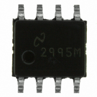
LP2995M/NOPB National Semiconductor, LP2995M/NOPB Datasheet - Page 10

LP2995M/NOPB
Manufacturer Part Number
LP2995M/NOPB
Description
IC REGULATOR DDR TERM 8-SOIC
Manufacturer
National Semiconductor
Datasheet
1.LP2995MRNOPB.pdf
(14 pages)
Specifications of LP2995M/NOPB
Applications
Converter, DDR
Voltage - Input
2.5 ~ 5.5 V
Number Of Outputs
1
Operating Temperature
0°C ~ 125°C
Mounting Type
Surface Mount
Package / Case
8-SOIC (3.9mm Width)
Primary Input Voltage
2.5V
No. Of Outputs
1
No. Of Pins
8
Output Current
1.5A
Operating Temperature Range
0°C To +125°C
Msl
MSL 1 - Unlimited
Filter Terminals
SMD
Rohs Compliant
Yes
Current Rating
1.5A
For Use With
LP2995M-EVAL - BOARD EVALUATION LP2995M
Lead Free Status / RoHS Status
Lead free / RoHS Compliant
Voltage - Output
-
Other names
*LP2995M
LP2995M
LP2995M
www.national.com
PCB Layout Considerations
1.
2.
3.
AVIN and PVIN should be tied together for optimal
performance. A local bypass capacitor should be placed
as close as possible to the PVIN pin.
GND should be connected to a ground plane with
multiple vias for improved thermal performance.
V
at the point where regulation is required. For
SENSE
should be connected to the V
TT
termination bus
10
4.
5.
motherboard applications an ideal location would be at
the center of the termination bus.
VDDQ can be connected remotely to the VDDQ rail input
at either the DIMM or the Chipset. This provides the most
accurate point for creating the reference voltage.
V
ceramic capacitor for improved performance. This
capacitor should be located as close as possible to the
V
REF
REF
should be bypassed with a 0.01 µF or 0.1 µF
pin.


