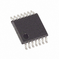
MAX3355EEUD+ Maxim Integrated Products, MAX3355EEUD+ Datasheet - Page 6

MAX3355EEUD+
Manufacturer Part Number
MAX3355EEUD+
Description
IC CHARGE PUMP USB OTG 14TSSOP
Manufacturer
Maxim Integrated Products
Datasheet
1.MAX3355EEUD.pdf
(11 pages)
Specifications of MAX3355EEUD+
Applications
Charge Pump, USB
Voltage - Input
2.6 ~ 5.5 V
Number Of Outputs
1
Operating Temperature
-40°C ~ 85°C
Mounting Type
Surface Mount
Package / Case
14-TSSOP
Maximum Operating Temperature
+ 85 C
Minimum Operating Temperature
- 40 C
Mounting Style
SMD/SMT
Lead Free Status / RoHS Status
Lead free / RoHS Compliant
Voltage - Output
-
Lead Free Status / Rohs Status
Lead free / RoHS Compliant
±15kV ESD-Protected USB On-the-Go
Charge Pump and Comparators in UCSP
6
UCSP
_______________________________________________________________________________________
A1
A2
A3
A4
B1
B2
B3
B4
C1
C2
C3
C4
—
PIN
TSSOP
7, 8
11
14
13
12
10
2
3
5
6
1
4
9
OTG SIE
OFFVBUS
STATUS1
STATUS2
µP
ID_OUT
NAME
SHDN
ID_IN
V
GND
N.C.
V
C+
BUS
V
C-
CC
V
L
CC
V
L
D+
D-
0.1µF
Power Supply. +2.6V to +5.5V input supply. Bypass V
Device ID Output. Output of ID_IN level translated to V
Status Output 1. Provides output voltage detection for use during HNP handshaking (Tables 1
and 2).
Status Output 2. Provides output voltage detection for use during HNP handshaking (Tables 1
and 2).
U S B S up p l y. V
V
b e b ackd r i ven to + 6.0V w i thout any conseq uence. Byp ass V
V
Shutdown. Connect SHDN to GND to enter shutdown and reduce supply current to less than
1µA. Connect SHDN to V
Logic Supply. V
between +1.65V and V
Charge-Pump Positive Connection
Charge-Pump Negative Connection
Ground
Device ID. ID_IN is internally pulled up to V
ID_IN to GND for device A.
No Connection
1µF
B U S
BUS
i s l ow er than + 2.1V w hen ID _IN i s op en or a l oad g r eater than 96.5µF i s sensed . V
Off. Turns the internal charge pump providing V
V
V
OFFVBUS
ID_OUT
STATUS1
STATUS2
SHDN
B U S
CC
L
L
sets the logic output high voltage and logic input high threshold. V
p r ovi d es a nom i nal + 5.0V outp ut w hen ID _IN i s l ow and O FFVBUS i s hi g h.
CC
MAX3355E
L
.
for normal operation.
ID_IN
V
GND
BUS
C+
C-
FUNCTION
CC
Typical Application Circuit
. Leave ID_IN open for device B and connect
C1
0.1µF
C
1µF
LOAD
CC
BUS
L
.
to GND with a 1µF capacitor.
on and off.
B U S
to G N D w i th a 1µF cap aci tor .
CONNECTOR
USB OTG
Pin Description
L
B U S
must be
can


