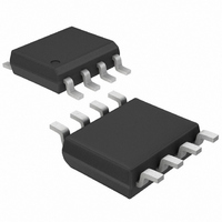
MAX1810ESA+ Maxim Integrated Products, MAX1810ESA+ Datasheet - Page 7

MAX1810ESA+
Manufacturer Part Number
MAX1810ESA+
Description
IC REG SMART NIC 8-SOIC
Manufacturer
Maxim Integrated Products
Datasheet
1.MAX1810ESA.pdf
(8 pages)
Specifications of MAX1810ESA+
Applications
Network, Telecom
Voltage - Input
4.5 ~ 5.5 V
Number Of Outputs
1
Voltage - Output
3.3V
Operating Temperature
-40°C ~ 85°C
Mounting Type
Surface Mount
Package / Case
8-SOIC (3.9mm Width)
Lead Free Status / RoHS Status
Lead free / RoHS Compliant
Thermal overload protection safeguards the MAX1810
in the event of fault conditions. For continuous opera-
tion, do not exceed the absolute maximum junction-
temperature rating of T
Both the MAIN and STBY regulators also feature over-
current protection nominally at 900mA. The AUX switch
is not current limited.
Maximum power dissipation of the MAX1810 depends
on the thermal resistance of the case and circuit board,
the temperature difference between the die junction
and ambient air, and the rate of airflow. The power dis-
sipation of the device is P = I
resulting maximum power dissipation is:
where T
(150°C) and T
thermal resistance from the die junction to the package
case, and θ
through the PC board, copper traces, and other materi-
als to the surrounding air (Figure 3). For optimum
power dissipation, use a large ground plane with good
thermal contact to pins 5 through 8. For multilayer
boards, multiple vias are recommended.
Figure 3. Power Operating Region: Maximum Output Current
vs. Supply Voltage
Operating Region and Power Dissipation
J(MAX)
P
1.6
1.4
1.2
1.0
0.8
0.6
0.4
0.2
MAX
0
CA
3.5
A
= ((T
is the thermal resistance from the case
is the maximum junction temperature
MAXIMUM CONTINUOUS CURRENT LIMIT
is the ambient temperature, θ
Network Interface Card Smart Regulator
_______________________________________________________________________________________
4.0
J(MAX)
SUPPLY VOLTAGE (V)
J
T
T
= +150°C.
J(MAX)
A
4.5
= +80°C
– T
= +150°C
A
T
A
5.0
) / (θ
OUT
= +70°C
T
A
= +50°C
JC
(V
5.5
IN
+ θ
– V
CA
6.0
))
OUT
JC
). The
is the
The MAX1810 requires a 1µF ceramic bypass capaci-
tor at OUT to maintain regulator stability (Figure 4).
When switching between input supplies, the MAX1810
may cause a voltage disturbance on either the MAIN or
STBY input. Limit this disturbance to below the hystere-
sis level (150mV) to guarantee precise switchover. If
the MAIN and STBY input supplies do not have filter
capacitance of their own near the MAX1810 inputs,
then bypass capacitors (2.2µF is recommended) may
be needed at MAIN and STBY. If the input supplies to
MAIN and STBY already have greater than 2.2µF of out-
put capacitance, then no additional capacitance is
required. Place input and output filter capacitors as
close to the device as possible to minimize the effect of
lead inductance of the PC board traces.
TRANSISTOR COUNT: 811
PROCESS: BiCMOS
Figure 4. Typical Application Circuit
*REQUIRED ONLY IF INPUT SUPPLIES DO NOT HAVE NEARBY OUTPUT CAPACITANCE.
+3.3V AUX
+5V MAIN
+5V STBY
INPUT
INPUT
INPUT
2.2µF
2.2µF
0.1µF
*
*
*
Applications Information
MAIN
STBY
AUX
MAX1810
Chip Information
Capacitor Selection
GND
OUT
C
1.0µF
OUT
OUT
+3.3V, 500mA
7


