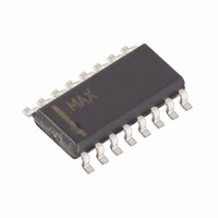
MAX848ESE+ Maxim Integrated Products, MAX848ESE+ Datasheet - Page 2

MAX848ESE+
Manufacturer Part Number
MAX848ESE+
Description
IC DC-DC CONV LN HP 16-SOIC
Manufacturer
Maxim Integrated Products
Datasheet
1.MAX848ESE.pdf
(16 pages)
Specifications of MAX848ESE+
Applications
Converter, RF Data Links
Voltage - Input
0.7 ~ 5.5 V
Number Of Outputs
1
Voltage - Output
3.3V, 2.7 ~ 5.5 V
Operating Temperature
0°C ~ 85°C
Mounting Type
Surface Mount
Package / Case
16-SOIC (3.9mm Width)
Lead Free Status / RoHS Status
Lead free / RoHS Compliant
ABSOLUTE MAXIMUM RATINGS
ON1, ON2, OUT, POUT to GND..................................-0.3V, +6V
PGND to GND ..........................................................-0.3V, +0.3V
LX to PGND ...............................................-0.3V, (V
CLK/SEL, DATA, POKIN, REF,
Continuous Power Dissipation (T
1-Cell to 3-Cell, High-Power,
Low-Noise, Step-Up DC-DC Converters
Stresses beyond those listed under “Absolute Maximum Ratings” may cause permanent damage to the device. These are stress ratings only, and functional
operation of the device at these or any other conditions beyond those indicated in the operational sections of the specifications is not implied. Exposure to
absolute maximum rating conditions for extended periods may affect device reliability.
ELECTRICAL CHARACTERISTICS
(V
unless otherwise noted.)
2
AINSEL, AIN1, AIN2, FB, POK to GND .....-0.3V, (V
Narrow SO (derate 8.7mW/°C above +70°C) ................696mW
Minimum Operating Voltage (Note 1)
REFERENCE
Reference Output Voltage
REF Load Regulation
REF Supply Rejection
DC-DC CONVERTER
Output Voltage (Note 2)
Output Current
FB Regulation Voltage
FB Input Current
Output Voltage Adjust Range
Output Voltage Lockout Range
Load Regulation (Note 4)
Minimum Start-Up Voltage (Note 5)
Frequency in Start-Up Mode
Operating Current in Shutdown
OUT
_______________________________________________________________________________________
= 3.6V, GND = PGND = CLK/SEL = ON1 =
PARAMETER
A
= +70°C)
I
-1µA < I
2.5V < V
V
Adjustable output, CLK/SEL = OUT
V
(Note 3)
CLK/SEL = OUT
I
V
Current into OUT pin, V
REF
LOAD
FB
FB
OUT
V
V
V
V
OUT
IN
IN
IN
< 0.1V, CLK/SEL = OUT
= 1.25V
= 0mA
= 1.5V
= 1.2V
= 2.4V
= 2.7V
< 1mA, T
REF
= 5V
OUT
POUT
ON2 = AINSEL = AIN1 = AIN2 = FB = POKIN, POUT = OUT, T
OUT
< 50µA
< 5V
+ 0.3V)
+ 0.3V)
CONDITIONS
A
> +25°C
MAX848, V
MAX849, V
V
V
V
V
V
V
OUT
OUT
OUT
OUT
OUT
OUT
ON2
= 3.3V
= 5V
= 3.3V
= 5V
= 3.3V
= 5V
= 3.6V
Operating Temperature Range
Junction Temperature ......................................................+150°C
Storage Temperature.........................................-65°C to +160°C
Lead Temperature (soldering, 10sec) .............................+300°C
IN
IN
MAX848ESE/MAX849ESE .................................-40°C to +85°C
= 3.3V
= 3.6V
MAX848
MAX849
MAX848
MAX849
MAX848
MAX849
MAX848
MAX849
MAX848
MAX849
MAX848
MAX849
1.215
1.23
3.17
MIN
2.7
2.1
40
1.240
1000
TYP
1.25
3.34
-1.6
110
300
200
200
750
130
500
250
600
150
800
300
0.7
0.2
0.9
70
5
4
1.265
MAX
1.27
3.40
A
200
300
5.5
2.4
1.1
15
20
5
= 0°C to +85°C,
UNITS
kHz
mV
mV
mA
mA
nA
µA
%
V
V
V
V
V
V
V


