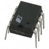
DPA423PN Power Integrations, DPA423PN Datasheet - Page 15

DPA423PN
Manufacturer Part Number
DPA423PN
Description
IC CONV DC-DC DPA SWITCH 8DIP
Manufacturer
Power Integrations
Series
DPA-Switch®r
Specifications of DPA423PN
Applications
Converter, Power Over Ethernet and Telecom Applications
Voltage - Input
16 ~ 75 V
Number Of Outputs
1
Voltage - Output
220V
Operating Temperature
-40°C ~ 125°C
Mounting Type
Through Hole
Package / Case
8-DIP (0.300", 7.62mm)
Output Voltage
9 V
Output Current
1.75 A
Input Voltage
- 0.3 V to + 220 V
Switching Frequency
282 KHz to 425 KHz
Operating Temperature Range
- 40 C to + 150 C
Mounting Style
Through Hole
Duty Cycle (max)
79 %
For Use With
596-1009 - KIT DESIGN ACCELERATOR DC-DC596-1007 - KIT DESIGN ACCELERATOR POE CONV
Lead Free Status / RoHS Status
Lead free / RoHS Compliant
Other names
596-1011-5
Available stocks
Company
Part Number
Manufacturer
Quantity
Price
Part Number:
DPA423PN
Manufacturer:
POWER
Quantity:
20 000
Figure 25. A High Efficiency 30 W, 5 V, Telecom Input DC-DC Converter.
High Efficiency 30 W Forward Converter
The circuit shown in Figure 25 is a typical implementation of a
single output DC-DC converter using DPA-Switch in a forward
configuration with synchronous rectification. This design
delivers 30 W at 5 V, from a 36 VDC to 75 VDC input with a
nominal efficiency at 48 VDC of 90% using the DPA425R.
By taking advantage of many of the built-in features of the
DPA-Switch, the design is greatly simplified compared to a
discrete implementation. Resistor R1 programs the input under-
voltage and overvoltage thresholds to typically 33 V and 86 V
respectively. This resistor also linearly reduces the maximum
duty from the internal maximum of 75% at 36 V to 42% at
72 V to prevent core saturation during load transients at high input
voltages. The DPA-Switch internal thresholds are toleranced
and characterized so the designer can guarantee the converter
will begin operation at 36 V, necessary to meet ETSI standards,
without the cost of an external reference IC.
The current limit is externally set by resistor R3 to just above the
drain current level needed for maximum load regulation to limit
the maximum overload power of the converter. The externally
programmable current limit feature also allows a larger
DPA-Switch family member to be selected. Using the X pin, the
current limit can be adjusted to the same level. A large device
reduces conduction losses and improves efficiency without
Application Examples
36-75 VDC
+
V
V
IN
IN
*Optional components
C1, C2 & C3
2.5 A
1 µH
100 V
1 µF
L1
SMBJ
VR1
150
D
619 kΩ
S
1%
R1
CONTROL
CONTROL
X
18.2 kΩ
L
1%
R3
F
C
DPA-Switch
U1
DPA425R
1.5 kV
1 nF
220 nF
C7
T1
C5
10 Ω
R17
10 Ω
R15
Si4888
10 Ω
R14
Q2
DY
C9*
68 µF
1.0 Ω
10 V
C6
R4
3300 pF
10 kΩ
R16
C17
D4
BAV19WS
R5*
Si4888
requiring any other circuit changes. This has been used here
to replace the DPA424R with a DPA425R.
The selectable 300/400 kHz switching frequency is set to 300 kHz
by connecting the FREQUENCY (F) pin to CONTROL (C).
DRAIN voltage clamping is provided by VR1, which keeps
the peak DRAIN voltage within acceptable limits. Transformer
core reset is provided by the gate capacitance of Q1 with R17
in series. Optional reset capacitance C9 with R5 can be added
if necessary to supplement the gate capacitance of Q1.
The output of the transformer is rectified using MOSFETs
to provide synchronous rectification. The UV/OV function,
together with the turns ratio of the transformer, defines the
maximum MOSFET gate voltage, allowing the very simple
gate drive arrangement, without the need for drive windings
or a drive IC. During primary on-time, capacitor C17 couples
charge through resistor R15 to drive the gate of the forward
MOSFET, Q2. Capacitor C17 provides a DC isolated drive for
Q2, preventing gate overstress on Q1 during power down. The
time constant formed by R16 and C17 is selected to be much
longer than one switching cycle. Diode D4 resets the voltage
on capacitor C17 before the next switching cycle. During the
primary off-time, the diode D2 provides a conduction path for
the energy in inductor L2 while Q1 is still off. The transformer
PC357N1T
DY
Q1
D2
U2
4.7 µF
20 V
C4
19WS
BAV
D1
L2
10 kΩ
10 µF
BAV19WS
LM431AIM3
10 V
R7
C13
D3
U3
150 Ω
U2
R6
100 µF
10 V
C10
100 µF
10 V
C11
100 nF
5.1 Ω
R12
C16
1 µF
C14
DPA423-426
10 V
1 µF
C12
10.0 kΩ
10.0 kΩ
220 Ω
R10
R11
1%
1%
R9
PI-3472-061704
7/05
5 V, 6 A
P
RTN
15


