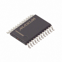
MAX1778EUG+ Maxim Integrated Products, MAX1778EUG+ Datasheet - Page 20

MAX1778EUG+
Manufacturer Part Number
MAX1778EUG+
Description
IC DCDC CONV MULTI OUT 24TSSOP
Manufacturer
Maxim Integrated Products
Datasheet
1.MAX1778EUG.pdf
(39 pages)
Specifications of MAX1778EUG+
Applications
Converter, TFT, LCD
Voltage - Input
2.7 ~ 5.5 V
Number Of Outputs
5
Voltage - Output
2.7 ~ 13 V
Operating Temperature
0°C ~ 85°C
Mounting Type
Surface Mount
Package / Case
24-TSSOP
Lead Free Status / RoHS Status
Lead free / RoHS Compliant
Quad-Output TFT LCD DC-DC
Converters with Buffer
Figure 2. Main Step-Up Converter Block Diagram
During normal pulse-width modulation (PWM) opera-
tion, the MAX1778/MAX1880–MAX1885 main step-up
controllers switch at a constant frequency of 500kHz or
1MHz (see Selector Guide), allowing the use of low-
profile inductors and output capacitors. Depending on
the input-to-output voltage ratio, the controller regulates
the output voltage and controls the power transfer by
modulating the duty cycle (D) of each switching cycle:
On the rising edge of the internal clock, the controller
sets a flip-flop when the output voltage is too low, which
turns on the N-channel MOSFET (Figure 2). The induc-
tor current ramps up linearly, storing energy in a mag-
netic field. Once the sum of the feedback voltage error
amplifier, slope-compensation, and current-feedback
signals trip the multi-input comparator, the MOSFET
turns off, the flip-flop resets, and the diode (D1) turns
on. This forces the current through the inductor to ramp
back down, transferring the energy stored in the mag-
netic field to the output capacitor and load. The MOS-
FET remains off for the rest of the clock cycle. Changes
20
______________________________________________________________________________________
D
COMPARATOR
≈
MAX1778
MAX1880
MAX1881
MAX1882
MAX1883
MAX1884
MAX1885
PWM
V
MAIN
Main Step-up Controller
V
MAIN
-
V
COMPARATOR
IN
AMPLIFIER
ERROR
ILIM
(80% DUTY)
S
R
OSC
INTG
C
Q
INTG
I
LIM
g
m
V
1.25V
REF
in the feedback voltage-error signal shift the switch-cur-
rent trip level, consequently modulating the MOSFET
duty cycle.
Under very light loads, an inherent switchover to pulse-
skipping takes place (Figure 3). When this occurs, the
controller skips most of the oscillator pulses in order to
reduce the switching frequency and gate charge loss-
es. When pulse-skipping, the step-up controller initiates
a new switching cycle only when the output voltage
drops too low. The N-channel MOSFET turns on, allow-
ing the inductor current to ramp up until the multi-input
comparator trips. Then, the MOSFET turns off and the
diode turns on, forcing the inductor current to ramp
down. When the inductor current reaches zero, the
diode turns off, so the inductor stops conducting cur-
rent. This forces the threshold between pulse-skipping
and PWM operation to coincide with the boundary
between continuous and discontinuous inductor-cur-
rent operation:
PGND
GND
I
REF
LOAD CROSSOVER
LX
FB
(
C
D1
REF
L1
R1
R2
(OPTIONAL)
R
V
V
COMP
MAIN
REF
)
= 1.25V
≈
C
C
= 1 +
IN
OUT
( )
2
1
R1
R2
(2.7V TO 5.5V)
(UP TO 13V)
⎛
⎜
⎝
V
V
V
MAIN
(OPTIONAL)
V
REF
MAIN
V
IN
C
IN
COMP
⎞
⎟
⎠
2
⎛
⎜
⎝
V
MAIN
f
OSC
-
L
V
IN
⎞
⎟
⎠


