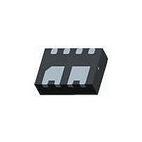
FAN1655MPX Fairchild Semiconductor, FAN1655MPX Datasheet - Page 2

FAN1655MPX
Manufacturer Part Number
FAN1655MPX
Description
IC REG LDO DDR BUS 3A 8+G5457MLP
Manufacturer
Fairchild Semiconductor
Datasheet
1.FAN1655MPX.pdf
(9 pages)
Specifications of FAN1655MPX
Applications
Controller, DDR
Voltage - Input
2.3 ~ 3.6 V
Number Of Outputs
1
Voltage - Output
1.1 ~ 1.8 V
Operating Temperature
0°C ~ 125°C
Mounting Type
Surface Mount
Package / Case
8-MLP
Polarity
Positive
Input Voltage Max
3.6 V
Output Voltage
1.15 V, 1.25 V, 1.35 V
Output Type
Selectable
Output Current
3 A
Load Regulation
40 mV
Maximum Operating Temperature
+ 125 C
Mounting Style
SMD/SMT
Minimum Operating Temperature
0 C
Reference Voltage
1.355 V
Lead Free Status / RoHS Status
Lead free / RoHS Compliant
Available stocks
Company
Part Number
Manufacturer
Quantity
Price
Company:
Part Number:
FAN1655MPX
Manufacturer:
FSC
Quantity:
15 000
Part Number:
FAN1655MPX
Manufacturer:
FAIRCHILD/ن»™ç«¥
Quantity:
20 000
FAN1655 Rev. 1.1.5
Pin Assignments
Pin Definitions
MLP
PAD
PAD
1, 4
2, 3
5
6
7
8
*Thermal impedance is measured with the power
pad soldered to a 0.5 square inch copper area.
The copper area should be connected to Vss
(ground) and positioned over an internal power
or ground plane to assist in heat dissipation.
VTTFORCE
VTTFORCE
VDD
VDD
VDD
VSS
VSS
VSS
16-Lead Plastic eTSSOP-16
eTSSOP
1, 2, 7
4, 5, 8
9, 16
PAD
Pin
3, 6
10
11
12
13
14
15
5
6
8
2
4
7
1
3
JC
= 4˚C/W*
FAN1655
SOIC-14
1, 2, 7
4, 5, 8
3, 6
10
11
12
13
14
9
16
15
14
13
12
11
10
VTTFORCE
VTTFORCE
9
as measured on FAN1655MP Eval Board
VTTFORCE
VTTSENSE
Pin Name
VREFOUT
VREFIN
VDDQ
NC
VDDQ
SHDN
VSSQ
VREFOUT
VSSQ
SHDN
VREFIN
VTTSENSE
NC
VDD
VSS
VDD
VDD
8-Lead MLP Package (5x6mm)
NC
JC
1
2
3
4
= 4˚C/W,
Input power for the LDO.
The VTT output voltage.
IC Ground.
Feedback for remote sense of the VTT voltage.
Alternative input for direct control of VTTOUT and
VREFOUT.
Shutdown. This active low shutdown turns off both VTT and
VREFOUT. This pin has an internal pull-down, and must be
externally driven high for the IC to be on.
Signal Ground.
Buffered Voltage Reference Output.
VDDQ Input. Attach this pin to the VDDQ supply to generate
VTT and VREFOUT.
No Internal Connection
Connect PAD to Vss Ground Plane
2
GND
JA
= 34˚C/W
8
7
6
5
VTTFORCE
VTTFORCE
VDDQ
VREFOUT
SHDN
VTTSENSE
VDD
VDD
VDD
VSS
VSS
JC
Pin Function
14-Lead Plastic SOIC
= 37˚C/W,
6
2
4
5
7
1
3
FAN1655M
JA
= 88˚C/W
14
13
12
11
10
9
8
www.fairchildsemi.com
VDDQ
VREFOUT
VSSQ
SHDN
VREFIN
VTTSENSE
VSS


