TC1267VETTR Microchip Technology, TC1267VETTR Datasheet
TC1267VETTR
Specifications of TC1267VETTR


Related parts for TC1267VETTR


TC1267VETTR Summary of contents
Page 1
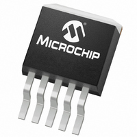
... TC1267VET 5-Pin DDPAK Pin Configuration 5-Pin DDPAK Tab is GND TC1267 2002 Microchip Technology Inc. © 400mA PCI LDO General Description The TC1267 is an application-specific, low dropout regulator (LDO), specifically intended for use in PCI peripheral card applications complying with PCI Power Management (PCI 2.0). It provides an uninterrupted, 3 ...
Page 2
... V ≤ 5.5V, 0mA ≤ I ≤ 400mA IN OUT 0mA ≤ I ≤ 400mA (Note 4) OUT V = 4. 0.1mA to 400mA OUT 4.3V ≤ V ≤ 5.5V 200µ < 200µA IN TH(LO) DR < thus avoiding D toggling during SOURCE HYST R 2002 Microchip Technology Inc. © ...
Page 3
... Recommended source impedance for 5V supply: ≤ 0.25Ω. This will ensure that detect threshold transitions Application Circuit, Figure 3-1. 5: See Timing Diagram, Figure 4-2. 6: Ground Current is independent of I LOAD 2002 Microchip Technology Inc. © (CONTINUED 3.3V 0.1mA 4.7µF, unless otherwise noted. Boldface IN AUX OUT ...
Page 4
... C1 C2 4.7µF 0.1µF NOTE: External switch (Q1): use Motorola MGSF1P02ELT1 or equivalent (PMOS, typical Gate Threshold Voltage = 1V, typical R DS21378B-page 4 Description Q1 TAB IS GND TC1267 C3 C4 0.1µF 4.7µF = 0.4Ω at VGS = 2.5V) DS(ON) 3.3V C5 0.1µF 2002 Microchip Technology Inc. © ...
Page 5
... Microchip Technology Inc. © Equation 4-1 can be used in conjunction with Equation 4-2 to ensure regulator thermal operation is within limits. For example: ...
Page 6
... DETECT THRESHOLD 3.65V D R rise and fall times (10 ≥ 100µsec. NOTE FIGURE 4-2: TIMING DIAGRAM 4. 3.65V D R rise and fall times (10 ≤ 0.1µsec. NOTE DS21378B-page 6 4.4V TH(HI 2.0V V HYST TH(LO) 2. 2.0V 2002 Microchip Technology Inc. © ...
Page 7
... V (V) AUX LDO Output Voltage vs. Junction Temperature 3. 200mA O 3. 3.32 3.31 3.30 3.29 3.28 3.27 3.26 -50 - JUNCTION TEMPERATURE °C 2002 Microchip Technology Inc. © I 0.45 +125° 0.40 V AUX 0.35 0.30 0.25 0.20 0.15 0.10 0.05 0. (Aux 0mA O 0 ...
Page 8
... V Falling voltage difference voltage OUT OUT DS(ON) difference from LDO to V supply AUX Trace 1: V – discharging a 1500µF capacitor IN Trace 2: D going low TH(LO) Trace offset 3.3V 3.14V OUT OUT(min 200µA LOAD 2002 Microchip Technology Inc. © ...
Page 9
... DDPAK .067 (1.70) .045 (1.14) .370 (9.40) .330 (8.38) .605 (15.37) .549 (13.95) PIN 1 .067 (1.70) TYP. 2002 Microchip Technology Inc. © PIN 1 User Direction of Feed P Standard Reel Component Orientation for TR Suffix Device (Mark Right Side Up) Pitch (P) Part Per Full Reel ...
Page 10
... TC1267 NOTES: DS21378B-page 10 2002 Microchip Technology Inc. © ...
Page 11
... The Microchip Worldwide Site (www.microchip.com) Please specify which device, revision of silicon and Data Sheet (include Literature #) you are using. New Customer Notification System Register on our web site (www.microchip.com/cn) to receive the most current information on our products. 2002 Microchip Technology Inc. TC1267 DS21378B-page 11 ...
Page 12
... TC1267 NOTES: DS21378B-page 12 2002 Microchip Technology Inc. ...
Page 13
... Serialized Quick Turn Programming (SQTP service mark of Microchip Technology Incorporated in the U.S.A. All other trademarks mentioned herein are property of their respective companies. © 2002, Microchip Technology Incorporated, Printed in the U.S.A., All Rights Reserved. Printed on recycled paper. Microchip received QS-9000 quality system ...
Page 14
... Korea Microchip Technology Korea 168-1, Youngbo Bldg. 3 Floor Samsung-Dong, Kangnam-Ku Seoul, Korea 135-882 Tel: 82-2-554-7200 Fax: 82-2-558-5934 Singapore Microchip Technology Singapore Pte Ltd. 200 Middle Road #07-02 Prime Centre Singapore, 188980 Tel: 65-6334-8870 Fax: 65-6334-8850 Taiwan Microchip Technology Taiwan 11F-3, No. 207 ...