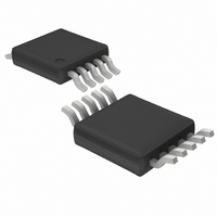
LT1947EMS Linear Technology, LT1947EMS Datasheet - Page 5

LT1947EMS
Manufacturer Part Number
LT1947EMS
Description
IC SW REG TFT-LCD TRPL ADJ10MSOP
Manufacturer
Linear Technology
Datasheet
1.LT1947EMSPBF.pdf
(12 pages)
Specifications of LT1947EMS
Applications
Converter, TFT, LCD
Voltage - Input
2.7 ~ 8 V
Number Of Outputs
3
Voltage - Output
Adjustable up to 30V
Operating Temperature
-40°C ~ 85°C
Mounting Type
Surface Mount
Package / Case
10-MSOP, Micro10™, 10-uMAX, 10-uSOP
Lead Free Status / RoHS Status
Contains lead / RoHS non-compliant
Available stocks
Company
Part Number
Manufacturer
Quantity
Price
Company:
Part Number:
LT1947EMS
Manufacturer:
LT
Quantity:
10 000
Part Number:
LT1947EMS
Manufacturer:
LT/凌特
Quantity:
20 000
Company:
Part Number:
LT1947EMS#PBF
Manufacturer:
MAX
Quantity:
4
Part Number:
LT1947EMS#PBF
Manufacturer:
LINEAR/凌特
Quantity:
20 000
Part Number:
LT1947EMS#TR
Manufacturer:
LINEAR/凌特
Quantity:
20 000
Part Number:
LT1947EMS#TRPBF
Manufacturer:
LINEAR/凌特
Quantity:
20 000
Company:
Part Number:
LT1947EMSE
Manufacturer:
LT
Quantity:
10 000
Part Number:
LT1947EMSE
Manufacturer:
LINEAR/凌特
Quantity:
20 000
PI FU CTIO S
FB1 (Pin 1): Feedback Pin for First Switcher. Connect
resistor divider tap here. Set AV
AV
FB2 (Pin 2): Feedback Pin for Second Switcher. Connect
resistor divider 2 here and set V
V
C
from C
reaching 1.26V to V
SW1 (Pin 4): AV
(see Figure 1). Minimize trace area at this pin to keep EMI
down.
GND (Pin 5): Ground. Connect directly to local ground
plane.
ON
T
(Pin 3): Timing Capacitor Pin. Connect a 10nF capacitor
DD
U
= 1.26V (1 + R3/R4) – 160mV.
= 1.26V(1 + R1/R2).
T
to ground to program a 2.3ms delay from FB1
U
DD
Switch Node. Connect L1 and D1 here
U
ON
turning on.
DD
according to:
ON
using:
V
ceramic capacitor close to the pin.
SW2 (Pin 7): V
Minimize trace area at this pin to keep EMI down.
SHDN (Pin 8): Pull this pin low for shutdown mode. For
normal operation, tie to a voltage between 2.4V and 8V.
V
connected to the emitter of Q3 (see Block Diagram), the
high side switch between V
V
Switcher. V
internal timer times out.
Exposed Pad (Pin 11): Ground (MSE package only). The
exposed pad must be soldered to the PCB and electrically
connected to ground.
IN
O2
ON
(Pin 6): Input Supply Pin. Must be bypassed with a
(Pin 9): SW2 Output. This node is also internally
(Pin 10): This is the delayed output for second
ON
reaches its programmed voltage after the
O2
Switch Node. Connect L2 and D2 here.
O2
and V
ON
.
LT1947
1947fa
5


