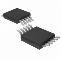
LT1947EMS#TR Linear Technology, LT1947EMS#TR Datasheet - Page 7

LT1947EMS#TR
Manufacturer Part Number
LT1947EMS#TR
Description
IC SW REG TFT-LCD TRPL ADJ10MSOP
Manufacturer
Linear Technology
Datasheet
1.LT1947EMSPBF.pdf
(12 pages)
Specifications of LT1947EMS#TR
Applications
Converter, TFT, LCD
Voltage - Input
2.7 ~ 8 V
Number Of Outputs
3
Voltage - Output
Adjustable up to 30V
Operating Temperature
-40°C ~ 85°C
Mounting Type
Surface Mount
Package / Case
10-MSOP, Micro10™, 10-uMAX, 10-uSOP
Lead Free Status / RoHS Status
Contains lead / RoHS non-compliant
Other names
LT1947EMSTR
Available stocks
Company
Part Number
Manufacturer
Quantity
Price
OPERATIO
To best understand operation of the LT1947, please refer
to the LT1947 Block Diagram. The device contains two
switching regulators, a timer and a high side switch. Three
outputs can be generated: an adjustable AV
charge-pumped inversion of the AV
and a time delayed adjustable output called V
V
connected to the C
The switching frequency of both switchers is 3MHz, set
internally. The switchers are current mode and are inter-
nally compensated. The main AV
limited at 1.1A, while the second V
350mA. They share the same 1.26V reference voltage.
When the input voltage is below approximately 2.7V, an
undervoltage lockout circuit disables switching.
When AV
holding the C
value, Q4 lets go of the C
source to charge the external capacitor, C
voltage on the C
connecting V
using the following formula:
ON
off for an externally set time interval, set by a capacitor
DD
is less than its final voltage, Q4 is turned on,
O2
T
pin at ground. When AV
to V
U
T
T
ON
pin.
pin reaches 1.28V, Q3 turns on,
. Capacitor value can be calculated
T
pin, allowing the 5.5µA current
GND
ON
V
DD
IN
C5
DD
Figure 2. Recommended Component Placement
AV
switcher is limited to
switcher is current
DD
output called V
L1
DD
D1
R1
reaches final
ON
T
DD
. When the
C6
. Q3 keeps
D3
output, a
C2
1
2
3
4
5
R3
R4
R2
OFF
C4
LT1947
D4
,
V
OFF
C1
10
A 10nF capacitor results in approximately 2.3ms of delay.
Layout Hints
The high speed operation of the LT1947 mandates careful
attention to layout for proper performance. Be sure to keep
input capacitor C1 as close as possible to the IC and
minimize trace area and length at the SW and FB pins.
Always use a ground plane under the switching regulator
to minimize interplane coupling. Figure 2 shows the rec-
ommended component placement.
The exposed pad of the MSE package must be soldered to
the PCB and electrically connected to ground. Thermal
vias to a large ground plane will lower the thermal resis-
tance.
Soft-Start
For applications requiring soft-start, a circuit consisting of
R
in Figure 3. For a combination of 33.2k/33nF, AV
to its final value in approximately 3ms.
9
8
7
6
SS
C3
C = (5.5µA • t
and C
V
IN
L2
GND
SS
V
ON
tied to the SHDN pin can be used, as shown
D2
DELAY
)/1.28V
1947 F02
SHDN
LT1947
DD
rises
1947fa
7


