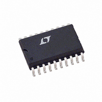
LTC1753CSW Linear Technology, LTC1753CSW Datasheet - Page 14

LTC1753CSW
Manufacturer Part Number
LTC1753CSW
Description
IC SW REG CNTRLR PENT III 20SOIC
Manufacturer
Linear Technology
Datasheet
1.LTC1753CGPBF.pdf
(24 pages)
Specifications of LTC1753CSW
Applications
Controller, Intel Pentium® III
Voltage - Input
5V
Number Of Outputs
1
Voltage - Output
1.3 ~ 3.5 V
Operating Temperature
0°C ~ 70°C
Mounting Type
Surface Mount
Package / Case
20-SOIC (7.5mm Width)
Lead Free Status / RoHS Status
Contains lead / RoHS non-compliant
Available stocks
Company
Part Number
Manufacturer
Quantity
Price
Company:
Part Number:
LTC1753CSW
Manufacturer:
LT
Quantity:
226
Part Number:
LTC1753CSW
Manufacturer:
LINEAR/凌特
Quantity:
20 000
Part Number:
LTC1753CSW#PBF
Manufacturer:
LINEAR/凌特
Quantity:
20 000
Part Number:
LTC1753CSW#TRPBF
Manufacturer:
LINEAR/凌特
Quantity:
20 000
APPLICATIO S I FOR ATIO
Table 4. Recommended MOSFETs for LTC1753 Applications
PARTS
Siliconix SUD50N03-10
D-PAK
Siliconix Si4410DY
SO-8
ON Semiconductor MTD20N03HDL
D PAK
Fairchild FDS6670A
SO-8
Fairchild FDS6680
SO-8
ON Semiconductor MTB75N03HDL
DD PAK
IR IRL3103S
DD PAK
IR IRLZ44
TO-220
Fuji 2SK1388
TO-220
Note: Please refer to the manufacturer’s data sheet for testing conditions
and detail information.
LTC1753
The R
be calculated by rearranging the relation P = I
P
efficiency or allowable thermal dissipation. A typical high
efficiency circuit designed with a 5V input and a 2.8V,
11.2A output might allow no more than 4% efficiency loss
at full load for each MOSFET. Assuming roughly 90%
efficiency at this current level, this gives a P
and a required R
14
MAX
R
R
[(2.8)(11.2A/0.9)(0.04)] = 1.39W per FET
DS ON Q
DS ON Q
DS(ON)
should be calculated based primarily on required
1
2
required for a given conduction loss can now
DC Q
DC Q
DS(ON)
P
U
P
MAX Q
MAX Q
1
2
of:
I
U
MAX
I
MAX
1
2
2
AT 25 C (m )
2
R
W
DS(ON)
7.5
19
20
35
10
14
28
37
V
8
V
V
IN
OUT MAX
IN
V
IN
P
MAX Q
V
I
P
OUT MAX
MAX
MAX Q
2
U
R.
value of:
1
RATED CURRENT (A)
2
I
2
11.5 at 25 C
10 at 100 C
16 at 100 C
59 at 100 C
40 at 100 C
36 at 100 C
15 at 25 C
10 at 25 C
20 at 25 C
13 at 25 C
75 at 25 C
56 at 25 C
50 at 25 C
35 at 25 C
8 at 75 C
2
Note also that while the required R
large MOSFETs, the dissipation numbers are only 1.39W
per device or less––large TO-220 packages and heat sinks
are not necessarily required in high efficiency applica-
tions. Siliconix Si4410DY or International Rectifier IRF7413
(both in SO-8) or Siliconix SUD50N03 or Motorola
MTD20N03HDL (both in D PAK) are small footprint sur-
face mount devices with R
of gate drive that work well in LTC1753 circuits. With
higher output voltages, the R
significantly lower than that for Q2. These conditions can
often be met by paralleling two MOSFETs for Q1 and using
a single device for Q2. Note that using a higher P
R
R
DS ON Q
DS ON Q
TYPICAL INPUT
CAPACITANCE
1
2
C
ISS
3200
2700
3200
2070
4025
1600
3300
1750
880
2 8
5
(pF)
5
V
V
V
5
V
1 39
2 8
11 2
DS(ON)
1 39
V
W
A
DS(ON)
11 2
W
2
JC
values below 0.03 at 5V
1.67
2.08
1.8
1.0
1.8
1.0
( C/W)
—
25
25
A
0 019
DS(ON)
of Q1 may need to be
2
0 025
values suggest
T
JMAX
MAX
175
150
150
150
150
150
175
175
150
( C)
value
1753fa


