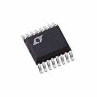
LTC3717EGN Linear Technology, LTC3717EGN Datasheet - Page 14

LTC3717EGN
Manufacturer Part Number
LTC3717EGN
Description
IC STEP-DWN CONTRLR SYNC 16-SSOP
Manufacturer
Linear Technology
Datasheet
1.LTC3717EGN.pdf
(20 pages)
Specifications of LTC3717EGN
Applications
Controller, DDR, QDR
Voltage - Input
4 ~ 36 V
Number Of Outputs
1
Voltage - Output
2 ~ 18 V
Operating Temperature
-40°C ~ 85°C
Mounting Type
Surface Mount
Package / Case
16-SSOP
Lead Free Status / RoHS Status
Contains lead / RoHS non-compliant
Available stocks
Company
Part Number
Manufacturer
Quantity
Price
Part Number:
LTC3717EGN
Manufacturer:
LT/凌特
Quantity:
20 000
Company:
Part Number:
LTC3717EGN#PBF
Manufacturer:
LT
Quantity:
416
Part Number:
LTC3717EGN#TRPBF
Manufacturer:
LT/凌特
Quantity:
20 000
APPLICATIO S I FOR ATIO
LTC3717
14
efficiency source, such as an output derived boost net-
work or alternate supply if available.
4. C
filtering the large RMS input current to the regulator. It
must have a very low ESR to minimize the AC I
sufficient capacitance to prevent the RMS current from
causing additional upstream losses in fuses or batteries.
Other losses, including C
conduction loss during dead time and inductor core loss
generally account for less than 2% additional loss.
When making adjustments to improve efficiency, the
input current is the best indicator of changes in efficiency.
If you make a change and the input current decreases, then
the efficiency has increased. If there is no change in input
current, then there is no change in efficiency.
Checking Transient Response
The regulator loop response can be checked by looking at
the load transient response. Switching regulators take
several cycles to respond to a step in load current. When
a load step occurs, V
equal to I
resistance of C
discharge C
the regulator to return V
During this recovery time, V
overshoot or ringing that would indicate a stability prob-
lem. The I
will provide adequate compensation for most applica-
tions. For a detailed explanation of switching control loop
theory see Application Note 76.
Design Example
As a design example, take a supply with the following
specifications: V
1.25V 5%, I
the timing resistor with V
and choose the inductor for about 40% ripple current at
the maximum V
R
IN
ON
loss. The input capacitor has the difficult job of
TH
( .
0 7
LOAD
OUT
pin external components shown in Figure 6
OUT(MAX)
1 25 2 5
V
.
generating a feedback error signal used by
)(
IN
OUT
(ESR), where ESR is the effective series
IN
250
:
V
U
= V
.
( .
OUT
kHz
REF
= 10A, f = 250kHz. First, calculate
I
LOAD
V
immediately shifts by an amount
OUT
)(
U
ON
OUT
– .
= 2.5V, V
10
0 7
ESR loss, Schottky diode D1
= V
pF
OUT
also begins to charge or
to its steady-state value.
V
OUT
) .
2 5
)
can be monitored for
W
:
V
EXTVCC
514
= 5V, V
k
2
U
R loss and
OUT
=
Selecting a standard value of 0.68 H results in a maximum
ripple current of:
Next, choose the synchronous MOSFET switch. Choosing
a Si4874 (R
Tying V
for a nominal value of 110mV with current limit occurring
at 143mV. To check if the current limit is acceptable,
assume a junction temperature of about 40 C above a
70 C ambient with
and double check the assumed T
Because the top MOSFET is on roughly the same amount
of time as the bottom MOSFET, the same Si4874 can be
used as the synchronous MOSFET.
The junction temperatures will be significantly less at
nominal current, but this analysis shows that careful
attention to heat sinking will be necessary in this circuit.
C
85 C. The output capacitors are chosen for a low ESR of
0.013 to minimize output voltage changes due to induc-
tor ripple current and load steps. For current sinking
applications where current flows back to the input through
the top transistor, output capacitors with a similar amount
of bulk C and ESR should be placed on the input as well.
P
JA
IN
BOT
V
T
I
L
LIMIT
= 40 C/W) yields a nominal sense voltage of:
J
is chosen for an RMS current rating of about 5A at
SNS(NOM)
I
L
= 70 C + (1.02W)(40 C/W) = 111 C
(
RNG
250
2 5
.
(
250
to 1.1V will set the current sense voltage range
( . )( .
V
kHz
1 4 0 010
2 5
DS(ON)
= (10A)(1.3)(0.0083 ) = 108mV
– .
1 25
.
kHz
143
.
1 25
)( . )(
1 25
V
.
0 4 10
)( .
V
mV
0 68
= 0.0083
V
V
110 C
( . ) ( . )( .
12 1
A
)
H
)
= 1.4:
A
)
1
2
1
1
2
( .
–
3 7
1 4 0 010
1 25
(NOM) 0.010
2 5
J
1 25
.
2 5
.
.
A
in the MOSFET:
.
V
)
V
V
V
12 1
.
0 63
3 7
.
A
)
.
A
sn3717 3717fs
1 02
H
.
(MAX),
W


