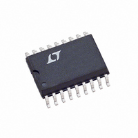
LTC1043CSW#TR Linear Technology, LTC1043CSW#TR Datasheet - Page 5

LTC1043CSW#TR
Manufacturer Part Number
LTC1043CSW#TR
Description
IC BUILDING BLK INST DUAL 18SOIC
Manufacturer
Linear Technology
Datasheet
1.LTC1043CNPBF.pdf
(16 pages)
Specifications of LTC1043CSW#TR
Applications
Instrumentation
Voltage - Input
3 ~ 18 V
Number Of Outputs
2
Operating Temperature
-40°C ~ 85°C
Mounting Type
Surface Mount
Package / Case
18-SOIC (7.5mm Width)
Lead Free Status / RoHS Status
Contains lead / RoHS non-compliant
Voltage - Output
-
Available stocks
Company
Part Number
Manufacturer
Quantity
Price
APPLICATIO S I FOR ATIO
Common Mode Rejection Ratio (CMRR)
The LTC1043, when used as a differential to single-ended
converter rejects common mode signals and preserves
differential voltages (Figure 1). Unlike other techniques,
the LTC1043’s CMRR does not degrade with increasing
common mode voltage frequency. During the sampling
mode, the impedance of Pins 2, 3 (and 11, 12) should be
reasonably balanced, otherwise, common mode signals
will appear differentially. The value of the CMRR depends
on the value of the sampling and holding capacitors
(C
common mode voltages are not sampled, the
common mode signal frequency can well exceed the
sampling frequency without experiencing aliasing
phenomena. The CMRR of Figure 1 is measured by
TEST CIRCUITS
S
, C
0V TO 10V
H
) and on the sampling frequency. Since the
+
+
(TEST PIN)
V +
+
Test Circuit 3. Oscillator Frequency, f
A
IV
(7, 13, 6, 18)
Test Circuit 1. Leakage Current Test
2
4
5
6
U
(11, 12, 2, 3)
LTC1043
U
(8, 14, 5, 15)
NOTE: TO OPEN SWITCHES,
W
V –
17
16
S1 AND S3
SHOULD BE CONNECTED
TO V – . TO OPEN S2, S4,
C
TO V + C
OSC
PIN SHOULD BE
C
LTC1043 • TC03
OSC
OSC
OSC
U
LTC1043 • TC01
Figure 1. Differential to Single-Ended Converter
+
V
V
CM
D
+
V
+
+
–
CMRR = 20 LOG
NOTE:
Test Circuit 4. CMRR Test
≤ V
V IN
13
7
C
Test Circuit 2. R
CM
S
CURRENT SOURCE
, C
13
10
≤ V
FOR OPTIMUM CMRR, THE C
BE LARGER THAN 0.0047µF, AND
THE SAMPLING CAPACITOR ACROSS
PINS 11 AND 12 SHOULD BE PLACED
OVER A SHIELD TIED TO PIN 10
7
H
(7, 13, 6, 18)
100µA to 1mA
ARE MYLAR OR POLYSTRENE
+
1/2 LTC1043
C
C
C
S
+
–
( )
11
12
V
V
11
12
OUT
CM
1µF
ON
A
14
8
(11, 12, 2, 3)
Test
V
D
14
LTC1043 • AI01
8
LTC1043 • TC02
OSC
+
(8, 14, 5, 15)
SHOULD
LTC1043
+
C
H
1µF
V
OUT
CAPACITORS ARE
NOT ELECTROLYTIC
LTC1043 • TC04
1043fa
5


