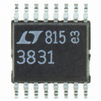
LTC3831EGN#PBF Linear Technology, LTC3831EGN#PBF Datasheet

LTC3831EGN#PBF
Specifications of LTC3831EGN#PBF
Available stocks
Related parts for LTC3831EGN#PBF
LTC3831EGN#PBF Summary of contents
Page 1
... The 200kHz free-running clock frequency can be externally adjusted or synchronized with an external signal from 100kHz to above 500kHz. In shutdown mode, the LTC3831 supply current drops to <10μA. L, LT, LTC and LTM are registered trademarks of Linear Technology Corporation. All other trademarks are the property of their respective owners. V DDQ 2 ...
Page 2
... Junction Temperature (Note 9) ............................. 125°C Operating Temperature Range Note 4) .....–40°C to 85°C Storage Temperature Range ...................–65°C to 150°C Lead Temperature (Soldering, 10 sec) .................. 300°C ORDER INFORMATION LEAD FREE FINISH TAPE AND REEL LTC3831EGN#PBF LTC3831EGN#TRPBF LTC3831IGN#PBF LTC3831IGN#TRPBF LEAD BASED FINISH TAPE AND REEL LTC3831EGN ...
Page 3
ELECTRICAL CHARACTERISTICS range, otherwise specifi cations are SYMBOL PARAMETER V Maximum V COMPMAX COMP /ΔI Frequency Adjustment Δf OSC FREQSET A Error Amplifi er Open-Loop DC Gain V g Error Amplifi er Transconductance m I Error Amplifi ...
Page 4
LTC3831 TYPICAL PERFORMANCE CHARACTERISTICS Load Regulation 1.270 T = 25°C A REFER TO FIGURE 1 1.265 NEGATIVE OUTPUT CURRENT INDICATES CURRENT SINKING 1.260 1.255 1.250 1.245 1.240 1.235 1.230 –4 – –6 0 OUTPUT CURRENT (A) 3831 G02 ...
Page 5
TYPICAL PERFORMANCE CHARACTERISTICS Maximum TG Duty Cycle vs Temperature 100 REFER TO FIGURE –50 – 100 TEMPERATURE (°C) 3831 G11 Output Current ...
Page 6
LTC3831 TYPICAL PERFORMANCE CHARACTERISTICS PV Supply Current CC vs Gate Capacitance 25° 12V CC1 CC1 GATE ...
Page 7
PIN FUNCTIONS FREQSET (Pin 11): Frequency Set. Use this pin to adjust the free-running frequency of the internal oscillator. With the pin fl oating, the oscillator runs at about 200kHz. A resistor from FREQSET to ground speeds up the oscillator; ...
Page 8
LTC3831 TEST CIRCUITS COMP 2.5V APPLICATIONS INFORMATION OVERVIEW The LTC3831 is a voltage mode feedback, synchronous switching regulator controller (see Block Diagram) de- signed for use in high to medium power, DDR memory termination. It ...
Page 9
APPLICATIONS INFORMATION back signal is greater than 3% above V two comparators from triggering due to noise, the MIN and MAX comparators’ response times are deliberately delayed by two to three microseconds. These two comparators help prevent extreme output perturbations ...
Page 10
LTC3831 APPLICATIONS INFORMATION and source pins. In addition, connect a 0.1μF decoupling capacitor across R to fi lter switching noise. Other- IMAX wise, noise spikes or ringing at Q1’s source can cause the actual current limit to be greater than ...
Page 11
APPLICATIONS INFORMATION SHDN 200kHz FREE RUNNING RAMP SIGNAL TRADITIONAL SYNC METHOD WITH EARLY RAMP TERMINATION RAMP AMPLITUDE ADJUSTED LTC3831 KEEPS RAMP AMPLITUDE CONSTANT UNDER SYNC Figure 4. External Synchronization Operation controller feedback loop result, the loop crossover frequency ...
Page 12
LTC3831 APPLICATIONS INFORMATION than 7V, a 12V zener diode should be included from PV to PGND to prevent transients from damaging the circuitry the gate of Q1. CC1 For applications with a lower V supply, a tripling ...
Page 13
APPLICATIONS INFORMATION 1μ 0.1μF SS 0.01μF + 130k 4.7μF FREQSET SHDN SHDN COMP 33pF 15k C C 1500pF Power MOSFETs Two N-channel power MOSFETs are required for most LTC3831 circuits. These should be selected ...
Page 14
LTC3831 APPLICATIONS INFORMATION output might allow no more than 3% effi ciency loss at full load for each MOSFET. Assuming roughly 90% effi ciency at this current level, this gives a P MAX (1.25V)(5A/0.9)(0.03) = 0.21W per FET and a ...
Page 15
APPLICATIONS INFORMATION capacitor values determine the transient recovery time. In general, a smaller value inductor improves transient response at the expense of ripple and inductor core satura- tion rating. A 2μH inductor has a 0.57A/μs rise time in this application, ...
Page 16
LTC3831 APPLICATIONS INFORMATION not for capacitance value. A capacitor with suitable ESR will usually have a larger capacitance value than is needed to control steady-state output ripple. Electrolytic capacitors, such as the Sanyo MV-WX series, rated for use in switching ...
Page 17
APPLICATIONS INFORMATION point changes with input voltage, load current variations, all suggest a more practical empirical method. This can be done by injecting a transient current at the load and using an RC network box to iterate toward the fi ...
Page 18
LTC3831 APPLICATIONS INFORMATION LAYOUT CONSIDERATIONS When laying out the printed circuit board, the following checklist should be used to ensure proper operation of the LTC3831. These items are also illustrated graphically in the layout diagram of Figure 10. The thicker ...
Page 19
... FLASH SHALL NOT EXCEED 0.010" (0.254mm) PER SIDE Information furnished by Linear Technology Corporation is believed to be accurate and reliable. However, no responsibility is assumed for its use. Linear Technology Corporation makes no representa- tion that the interconnection of its circuits as described herein will not infringe on existing patent rights. ...
Page 20
... Wide V Step-Down Controller for DDR Memory Termination IN LTC3718 Bus Termination Supply for Low Voltage V LTC3832 High Power Synchronous Switching Regulator Controller trademark of Linear Technology Corporation. SENSE 20 Linear Technology Corporation 1630 McCarthy Blvd., Milpitas, CA 95035-7417 (408) 432-1900 FAX: (408) 434-0507 ● COMMENTS SO-8 with Current Limit ...


