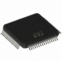
L6713A STMicroelectronics, L6713A Datasheet - Page 50

L6713A
Manufacturer Part Number
L6713A
Description
IC CTRLR 2/3PH W/DRIVERS 64-TQFP
Manufacturer
STMicroelectronics
Datasheet
1.L6713ATR.pdf
(64 pages)
Specifications of L6713A
Applications
Controller, Intel VR10, VR11, AMD CPU
Voltage - Input
12V
Number Of Outputs
3
Voltage - Output
0.3 ~ 1.6 V
Operating Temperature
0°C ~ 70°C
Mounting Type
Surface Mount
Package / Case
64-TQFP Exposed Pad, 64-eTQFP, 64-HTQFP, 64-VQFP
Output Current
2 A
Mounting Style
SMD/SMT
Maximum Operating Temperature
+ 125 C
Minimum Operating Temperature
0 C
Lead Free Status / RoHS Status
Lead free / RoHS Compliant
Available stocks
Company
Part Number
Manufacturer
Quantity
Price
Oscillator
19
50/64
Oscillator
L6713A embeds two/three phase oscillator with optimized phase-shift (180º/120º phase-
shift) in order to reduce the input rms current and optimize the output filter definition.
The internal oscillator generates the triangular waveform for the PWM charging and
discharging with a constant current an internal capacitor. The switching frequency for each
channel, F
load side results in being multiplied by N (number of phases).
The current delivered to the oscillator is typically 25 μA (corresponding to the free running
frequency F
between the OSC pin and SGND or VCC (or a fixed voltage greater than 1.24 V). Since the
OSC pin is fixed at 1.24 V, the frequency is varied proportionally to the current sunk (forced)
from (into) the pin considering the internal gain of 6 KHz/μA.
In particular connecting R
pin), while connecting R
the pin), according the following relationships:
R
R
Maximum programmable switching frequency per phase must be limited to 1 MHz to avoid
minimum Ton limitation. Anyway, device power dissipation must be checked prior to design
high switching frequency systems.
Figure 24. R
6
kHz
---------- -
OSC
OSC
μA
kHz
---------- -
μA
7000
6000
5000
4000
3000
2000
1000
0
25
=
vs. SGND
vs. +12V
=
200 kHz
200 kHz
SW
50
(
(
SW
, is internally fixed at 200 kHz so that the resulting switching frequency at the
OSC
= 200 kHz) and it may be varied using an external resistor (R
F
)
75
)
SW
–
6.456 10
---------------------------- -
+
R
vs. switching frequency
Fsw [kHz] Programmed
OSC
7.422 10
---------------------------- -
R
F
=
OSC
SW
100
200 kHz
(
⋅
kΩ
OSC
=
(
⋅
(
OSC
kΩ
200 kHz
4
)
125
⇒
to VCC = 12 V the frequency is reduced (current is forced into
3
)
(
⇒
to SGND the frequency is increased (current is sunk from the
)
R
–
OSC
150
R
12V 1.240V
----------------------------------- -
R
OSC
)
+
OSC
(
kΩ
–
--------------------------- - 6
R
175
(
kΩ
1.240V
OSC
(
)
kΩ
=
)
(
=
----------------------------------------------------------- -
200 kHz
200
)
kΩ
----------------------------------------------------------- -
F
⋅
SW
)
(
8kHz
------------- -
⋅
μA
8.608 10
400
350
300
250
200
150
100
(
50
kHz
0
7.422 10
kHz
---------- -
150
μA
) F
–
=
) 200 kHz
⋅
200 kHz
=
250
–
SW
⋅
200 kHz
4
(
(
350
3
kHz
(
(
)
)
450
–
[
Fsw [kHz] Programmed
kΩ
)
8.608 10
---------------------------- -
)
R
[
+
kΩ
OSC
]
550
7.422 10
---------------------------- -
R
]
OSC
(
⋅
kΩ
650
(
⋅
4
kΩ
)
⇒
OSC
750
3
)
R
⇒
OSC
) connected
850
R
OSC
(
L6713A
kΩ
950
(
)
kΩ
=
1050
--
2
)
=


