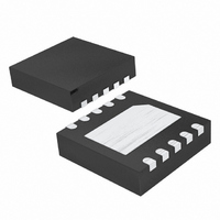
MAX8794ETB+T Maxim Integrated Products, MAX8794ETB+T Datasheet - Page 2

MAX8794ETB+T
Manufacturer Part Number
MAX8794ETB+T
Description
IC DDR LINEAR REG 10-TDFN
Manufacturer
Maxim Integrated Products
Datasheet
1.MAX8794ETBT.pdf
(13 pages)
Specifications of MAX8794ETB+T
Applications
Converter, DDR
Voltage - Input
1.1 ~ 3.6 V
Number Of Outputs
1
Voltage - Output
0.5 ~ 1.5 V
Operating Temperature
-40°C ~ 85°C
Mounting Type
Surface Mount
Package / Case
10-TDFN Exposed Pad
Lead Free Status / RoHS Status
Lead free / RoHS Compliant
ABSOLUTE MAXIMUM RATINGS
IN to PGND............................................................-0.3V to +4.3V
OUT to PGND ..............................................-0.3V to (V
OUTS to AGND ............................................-0.3V to (V
V
REFIN, REFOUT, SHDN, PGOOD to AGND...-0.3V to (V
PGND to AGND .....................................................-0.3V to +0.3V
REFOUT Short Circuit to AGND .................................Continuous
OUT Continuous RMS Current
ELECTRICAL CHARACTERISTICS
(V
Typical values are at T
Low-Voltage DDR Linear Regulator
Stresses beyond those listed under “Absolute Maximum Ratings” may cause permanent damage to the device. These are stress ratings only, and functional
operation of the device at these or any other conditions beyond those indicated in the operational sections of the specifications is not implied. Exposure to
absolute maximum rating conditions for extended periods may affect device reliability.
2
Input Voltage Range
Quiescent Supply Current (V
Shutdown Supply Current (V
Quiescent Supply Current (V
Shutdown Supply Current (V
Feedback-Voltage Error
Load-Regulation Error
Line-Regulation Error
OUTS Input Bias Current
OUTPUT
Output Adjust Range
OUT On-Resistance
Output Current Slew Rate
OUT Power-Supply Rejection
Ratio
OUT to OUTS Resistance
Discharge MOSFET On-
Resistance
CC
IN
100s ................................................................................±1.6A
1s ....................................................................................±2.5A
_______________________________________________________________________________________
to AGND.........................................................-0.3V to +4.3V
= 1.8V, V
PARAMETER
CC
= 3.3V, V
A
= +25°C.) (Note 1)
REFIN
CC
IN
CC
IN
)
)
)
)
= V
R
I
SYMBOL
DISCHARGE
I
CC(SHDN)
OUTS
IN(SHDN)
R
V
I
PSRR
OUTS
V
OUTS
I
OUTS
V
I
CC
CC
IN
IN
= 1.25V, SHDN = V
Power input
Bias supply
Load = 0, V
SHDN = AGND, V
SHDN = AGND, REFIN = AGND
Load = 0
SHDN = AGND
REFIN to OUTS,
I
-1A ≤ I
1.4V ≤ V
High-side MOSFET (source) (I
Low-side MOSFET (sink) (I
C
10Hz < f < 10kHz, I
C
SHDN = AGND
OUT
OUT
OUT
CC
IN
IN
= ±200mA
+ 0.3V)
+ 0.3V)
= 100µF, I
= 100µF
+ 0.3V)
OUT
IN
≤ 3.3V, I
≤ +1A
REFIN
CC
CONDITIONS
, circuit of Figure 1, T
OUT
> 0.45V
REFIN
OUT
OUT
Continuous Power Dissipation (T
Operating Temperature Range
Junction Temperature ......................................................+150°C
Storage Temperature Range .............................-65°C to +150°C
Lead Temperature (soldering, 10s) .................................+300°C
Soldering Temperature (reflow) .......................................+260°C
= 0.1A to 2A
10-Pin 3mm x 3mm TDFN
(derated 24.4mW/°C above +70°C)...........................1951mW
MAX8794ETB...................................................-40°C to +85°C
T
T
= ±100mA
> 0.45V
= 200mA,
A
A
= +25°C
= -40°C to +85°C
OUT
OUT
= -0.1A)
= 0.1A)
A
= -40°C to +85°C, unless otherwise noted.
MIN
1.1
2.7
-15
0.5
-4
-6
-1
A
= +70°C)
TYP
0.10
0.10
350
0.7
0.4
0.1
50
80
12
0
1
3
8
0.169
MAX
0.20
+15
600
100
3.6
3.6
1.3
1.5
+4
+6
+1
10
10
UNITS
A/µs
mA
mA
mV
mV
mV
µA
µA
µA
dB
kΩ
Ω
Ω
V
V


