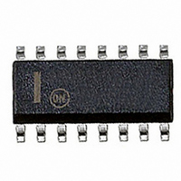
CS5165AGDWR16G ON Semiconductor, CS5165AGDWR16G Datasheet - Page 12

CS5165AGDWR16G
Manufacturer Part Number
CS5165AGDWR16G
Description
IC CTRLR BUCK SYNC 5BIT 16-SOIC
Manufacturer
ON Semiconductor
Datasheet
1.CS5165AGDWR16G.pdf
(18 pages)
Specifications of CS5165AGDWR16G
Applications
Controller, Intel Pentium® II
Voltage - Input
8 ~ 14 V
Number Of Outputs
2
Voltage - Output
1.34 ~ 2.09 V, 2.14 ~ 3.54 V
Operating Temperature
0°C ~ 70°C
Mounting Type
Surface Mount
Package / Case
16-SOIC (0.300", 7.5mm Width)
Mounting Style
SMD/SMT
Lead Free Status / RoHS Status
Lead free / RoHS Compliant
Available stocks
Company
Part Number
Manufacturer
Quantity
Price
Part Number:
CS5165AGDWR16G
Manufacturer:
ON/安森美
Quantity:
20 000
remain in this state until the overvoltage condition ceases or the
input voltage is pulled low. The bottom FET and board trace
must be properly designed to implement the OVP function.If
a dedicated OVP output is required, it can be implemented
using the circuit in Figure 22. In this figure the OVP signal will
go high (overvoltage condition), if the output voltage (V
exceeds 20% of the voltage set by the particular DAC code and
provided that PWRGD is low. It is also required that the
overvoltage condition be present for at least the PWRGD delay
time for the OVP signal to be activated. The resistor values
shown in Figure 22 are for V
The V
following equation:
Figure 21. OVP Response to an Input−to−Output Short
Trace 4− 5.0 V from PC Power Supply (5.0 V/div.)
Trace 1− Regulator Output Voltage (1.0 V/div.)
Trace 2− Inductor Switching Node 5.0 V/div.)
Trace 4− 5.0 V from PC Power Supply (2.0 V/div.)
Trace 1− Regulator Output Voltage (1.0 V/div.)
Cycle, Crow−Barring the Input Voltage to Ground
Figure 20. OVP Response to an Input−to−Output
Short Circuit by Immediately Providing 0% Duty
Circuit by Pulling the Input Voltage to Ground
OVP
(overvoltage trip−point) can be set using the
V OVP + V BEQ3 1 ) R2
M 5.00 ms
M 10.0 ms
DAC
= +2.8 V (DAC = 10111).
R1
http://onsemi.com
CORE
CS5165A
)
12
Output Enable Circuit
regulator output voltage, and is consistent with TTL DC
specifications. It is internally pulled−up. If pulled low (below
0.8 V), the output voltage is disabled. At the same time the
Power Good and Soft−Start pins are pulled low, so that when
normal operation resumes power−up of the CS5165A goes
through the Soft−Start sequence. Upon pulling the Enable pin
low, the internal IC bias is completely shut off, resulting in
total shutdown of the Controller IC.
Power Good Circuit
consistent with TTL DC specifications. It is externally
pulled−up, and is pulled low (below 0.3 V) when the regulator
output voltage typically exceeds ± 8.5% of the nominal output
voltage. Maximum output voltage deviation before Power
Good is pulled low is ± 12%.
The Enable pin (pin 8) is used to enable or disable the
The Power Good pin (pin 13) is an open−collector signal
Trace 2− PWRGD (2.0 V/div.)
Trace 4− V
Figure 22. Circuit To Implement A Dedicated OVP
Figure 23. PWRGD Signal Becomes Logic High as
CS5165A
V
OUT
PWRGD
Enters −8.5% of Lower PWRGD Threshold,
OUT
(1.0 V/div.)
+5.0 V
V
Output Using The CS5165A
OUT
10 k
= +2.84 V (DAC = 10111)
Q1
2N3906
10 k
+5.0 V
5.0 k
20 k
Q2
2N3904
56 k
15 k
V
CORE
R1
R2
Q3
2N3906
10 K
OVP


