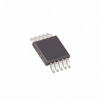
MAX1820XEUB+T Maxim Integrated Products, MAX1820XEUB+T Datasheet - Page 5

MAX1820XEUB+T
Manufacturer Part Number
MAX1820XEUB+T
Description
IC REG BUCK WCDMA 10-MSOP
Manufacturer
Maxim Integrated Products
Datasheet
1.MAX1821EUBT.pdf
(18 pages)
Specifications of MAX1820XEUB+T
Applications
Converter, WCDMA Power Amplifier Applications
Voltage - Input
2.6 ~ 5.5 V
Number Of Outputs
1
Voltage - Output
0.4 ~ 3.4 V
Operating Temperature
0°C ~ 85°C
Mounting Type
Surface Mount
Package / Case
10-MSOP, Micro10™, 10-uMAX, 10-uSOP
Lead Free Status / RoHS Status
Lead free / RoHS Compliant
ELECTRICAL CHARACTERISTICS (continued)
(V
(Notes 2, 3)
Note 2: Limits are 100% production tested at T
Note 3: Specifications to -40°C are guaranteed by design and not subject to production test.
(T
LX Leakage Current
Maximum Duty Cycle
Minimum Duty Cycle
SYNC AND OSCILLATOR
SYNC Divide Ratio
(MAX1820X)
SYNC Capture Range
(MAX1820X)
SYNC Divide Ratio
(MAX1820Y)
SYNC Capture Range
(MAX1820Y)
SYNC Leakage Current
Internal Oscillator Frequency
(MAX1820Z, MAX1821)
LOGIC INPUTS (SKIP, SHDN)
Logic Input High
Logic Input Low
Logic Input Current
BATT
A
100
= +25°C, unless otherwise noted.)
90
80
70
60
50
40
= 3.6V, SHDN = BATT, SKIP = SYNC = GND, V
0
guaranteed by design and characterization but are not production tested.
R
EFFICIENCY vs. OUTPUT VOLTAGE
PARAMETER
LOAD
0.5
(NORMAL MODE, V
= 5
1.0
OUTPUT VOLTAGE (V)
1.5
R
LOAD
_______________________________________________________________________________________
2.0
= 15
R
LOAD
2.5
IN
= 3.6V)
= 10
3.0
3.5
SYMBOL
duty
duty
I
f
SYNC
OSC
V
4.0
I
V
LX
IH
IL
MAX
MIN
A
WCDMA Cellular Phone 600mA
100
= +25°C for UCSP parts. Limits over the entire operating temperature range are
90
80
70
60
50
40
V
SKIP = GND
SKIP = BATT, V
S Y N C = si ne w ave, S Y N C i np ut = 200m V
S Y N C = si ne w ave, S Y N C i np ut = 800m V
SYNC = sine wave, AC-coupled,
SYNC input = 500mV
S Y N C = si ne w ave, S Y N C i np ut = 200m V
S Y N C = si ne w ave, S Y N C i np ut = 800m V
SYNC = sine wave, AC-coupled,
SYNC input = 500mV
V
V
M AX 1821X )
SYNC = GND
BATT
SYNC
SYNC
0
R
EFFICIENCY vs. OUTPUT VOLTAGE
LOAD
0.5
REF
= 5.5V, LX = GND or BATT
= IV ( M AX 1820Z , M AX 1821)
= IV ( M AX 1820X , M AX 1820Y , and
(PWM MODE, V
= 5
1.0
= 1.25V (MAX1820 only), T
OUTPUT VOLTAGE (V)
1.5
CONDITIONS
BATT
R
LOAD
2.0
= 15
= 4.2V
P-P
P-P
Typical Operating Characteristics
R
IN
LOAD
2.5
= 3.6V)
= 10
3.0
3.5
4.0
Buck Regulators
A
P-P
P-P
P-P
P-P
= -40°C to +85°C, unless otherwise noted.)
100
90
80
70
60
50
40
30
20
10
0
MIN
100
2.0
0.8
1.6
13
13
10
18
18
15
-1
-1
-5
EFFICIENCY vs. INPUT VOLTAGE
2.5
NORMAL MODE, R
V
OUT
V
OUT
3.0
= 1.8V
= 0.4V
3.5
V
IN
4.0
(V)
V
MAX
OUT
1.2
0.4
+1
+5
LOAD
10
13
13
16
18
18
21
4.5
1
0
1
= 3.4V
= 10
5.0
UNITS
Hz/Hz
Hz/Hz
5.5
MHz
MHz
MHz
µA
µA
µA
%
%
V
V
6.0
5


