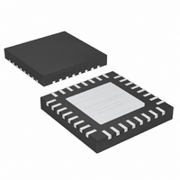
MAX1565ETJ+T Maxim Integrated Products, MAX1565ETJ+T Datasheet - Page 18

MAX1565ETJ+T
Manufacturer Part Number
MAX1565ETJ+T
Description
IC DGTL CAM PWR-SUP 5CH 32TQFN
Manufacturer
Maxim Integrated Products
Datasheet
1.MAX1565ETJT.pdf
(26 pages)
Specifications of MAX1565ETJ+T
Applications
Converter Controller, Digital Cameras
Voltage - Input
0.7 ~ 5.5 V
Number Of Outputs
5
Voltage - Output
3.3V, 1.25 ~ 5.5 V
Operating Temperature
-40°C ~ 85°C
Mounting Type
Surface Mount
Package / Case
32-TQFN Exposed Pad
Lead Free Status / RoHS Status
Lead free / RoHS Compliant
The output capacitor keeps output ripple small and
ensures control-loop stability. The output capacitor
must also have low impedance at the switching fre-
quency. Ceramic, polymer, and tantalum capacitors
are suitable, with ceramic exhibiting the lowest ESR
and high-frequency impedance.
Output ripple with a ceramic output capacitor is
approximately:
If the capacitor has significant ESR, the output ripple
component due to capacitor ESR is:
Output capacitor specifics are also discussed in the
Step-Up Compensation section and the Step-Down
Compensation section.
The external components required for the step-up are
an inductor, input and output filter capacitor, and com-
pensation RC. Typically, the inductor is selected to
operate with continuous current for best efficiency. An
exception might be if the step-up ratio, (V
greater than 1/(1 - D
PWM duty factor of 80%.
When using the step-up channel to boost from a low input
voltage, loaded startup is aided by connecting a
Schottky diode from the battery to OUTSU. See the
Minimum Startup Voltage vs. Load Current graph in the
Typical Operating Characteristics.
In most step-up designs, a reasonable inductor value
(L
which sets continuous peak-to-peak inductor current at
one-half the DC inductor current:
where D is the duty factor given by:
Given L
rent is 0.5 I
I
than L
However, if much smaller values are used, the inductor
current rises and a larger output capacitance may be
required to suppress output ripple.
Small, High-Efficiency, Five-Channel
Digital Still Camera Power Supply
18
IND(PK)
IDEAL
______________________________________________________________________________________
L
IDEAL
IDEAL
) can be derived from the following equation,
IDEAL
= 1.25 I
V
RIPPLE
OUT
, the consistent peak-to-peak inductor cur-
= [2 V
V
can be used to reduce inductor size.
RIPPLE(ESR)
OUT
Step-Up Component Selection
/(1 - D). The peak inductor current,
= I
D = 1 - (V
IN(MAX)
L(PEAK)
MAX
/ (1 - D). Inductance values smaller
), where D
= I
D(1 - D)] / (I
IN
[1/(2π f
L(PEAK)
/ V
OUT
OSC
MAX
)
Step-Up Inductor
ESR
OUT
C
is the maximum
OUT
OUT
f
OSC
)]
/V
)
IN
), is
The inductor and output capacitor are usually chosen
first in consideration of performance, size, and cost. The
compensation resistor and capacitor are then chosen to
optimize control-loop stability. In some cases it may help
to readjust the inductor or output capacitor value to get
optimum results. For typical designs, the component
values in the circuit of Figure 1 yield good results.
The step-up converter employs current-mode control,
thereby simplifying the control-loop compensation.
When the converter operates with continuous inductor
current (typically the case), a right-half-plane zero
(RHPZ) appears in the loop-gain frequency response.
To ensure stability, the control-loop gain should
crossover (drop below unity gain) at a frequency (f
much less than that of the right-half-plane zero.
The relevant characteristics for step-up channel com-
pensation are:
1) Transconductance (from FBSU to COMPSU), gm
2) Current-sense amplifier transresistance, R
3) Feedback regulation voltage, V
4) Step-up output voltage, V
5) Output load equivalent resistance, R
The key steps for step-up compensation are:
For continuous conduction, the right-plane zero fre-
quency (f
where D = the duty cycle = 1 - (V
inductor value, and I
rent. Typically target crossover (f
For example, if we assume V
and I
L = 3.3µH then:
1) Place f
2) Select R
3) Calculate the output filter capacitor (C
4) Determine if C
f
RHPZ
(135µS)
(0.3V/A)
in Ω = V
sient. R
corresponds to load current step.
required to allow the R
10pF).
OUT
= 3.35 (2/3.35)
f
RHPZ
RHPZ
C
= 0.5A, then R
C
SUOUT
sufficiently below the RHPZ and calculate C
C
sets a voltage delta on the COMP pin that
) is given by:
= V
based on the allowed load-step tran-
OUTSU
/I
P
LOAD
2
LOAD
is required (if calculated to be >
/ (2π x 4.7 x 10
(1 - D)
C
LOAD
is the maximum output cur-
and C
SUOUT
Step-Up Compensation
IN
2
/ (2π L I
= 6.7Ω. If we select
= 2V, V
C
C
FB
) for 1/6 the RHPZ.
, in V
selected.
IN
-6
(1.25V)
/V
x 0.5) = 115kHz
LOAD
OUT
OUT
), L is the
)
= 3.35V,
LOAD
OUT
CS
EA
C
C
.
)
)
,
,


