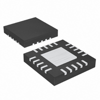
MAX8758ETG+T Maxim Integrated Products, MAX8758ETG+T Datasheet - Page 14

MAX8758ETG+T
Manufacturer Part Number
MAX8758ETG+T
Description
IC REG STEP UP 24-TQFN
Manufacturer
Maxim Integrated Products
Datasheet
1.MAX8758ETGT.pdf
(20 pages)
Specifications of MAX8758ETG+T
Applications
Converter, TFT, LCD
Voltage - Input
1.8 ~ 5.5 V
Number Of Outputs
1
Voltage - Output
5V
Operating Temperature
0°C ~ 85°C
Mounting Type
Surface Mount
Package / Case
24-TQFN Exposed Pad
Lead Free Status / RoHS Status
Lead free / RoHS Compliant
Activate the first mode by connecting MODE to LDO.
When CTL is logic high, Q1 turns on and Q2 turns off,
connecting GON to SRC. When CTL is logic low, Q1
turns off and Q2 turns on, connecting GON to DRN.
GON can then be discharged through a resistor con-
nected between DRN and PGND or AV
and stops discharging GON when V
times the voltage on THR.
When V
block works in the second mode. The rising edge of
V
SRC. An internal n-channel MOSFET Q3 between
MODE and GND is also turned on to discharge an
external capacitor between MODE and GND. The
falling edge of V
current source starts charging the MODE capacitor.
Once V
block turns off Q1 and turns on Q2, connecting GON to
DRN. GON can then be discharged through a resistor
connected between DRN and GND or AV
off and stops discharging GON when V
times the voltage on THR.
The timing of enabling the switch control block can be
adjusted with an external capacitor connected between
DLP and GND. An internal current source starts charg-
ing the DLP capacitor if the input voltage is above
1.75V (typ), SHDN is high, and the fault latch is not set.
The voltage on DLP linearly rises because of the con-
stant-charging current. When VDLP goes above 2.5V
(typ), the switch control block is enabled. The switch
control block is disabled and DLP is held low when the
MAX8758 is shut down or in a fault state.
The MAX8758 includes an internal 5V linear regulator.
OUT is the input of the linear regulator and should be
directly connected to the output of the step-up regulator.
The input voltage range is between 4.5V and 13V. The
output of the linear regulator (LDO) is set to 5V (typ). The
regulator powers all the internal circuitry including the
gate driver. This feature significantly improves the effi-
ciency at low input voltages. Bypass the LDO pin to
GND with a 0.22µF or greater ceramic capacitor.
Step-Up Regulator with Switch Control
and Operational Amplifier for TFT LCD
14
CTL
______________________________________________________________________________________
turns on Q1 and turns off Q2, connecting GON to
MODE
MODE
is less than 0.9 x V
exceeds 0.5 x V
CTL
turns off Q3, and an internal 50µA
Linear Regulator (LDO)
REF
LDO
, the switch control
, the switch control
GON
GON
DD
. Q2 turns off
DD
reaches 10
reaches 10
. Q2 turns
The inductance value, peak-current rating, and series
resistance are factors to consider when selecting the
inductor. These factors influence the converter’s effi-
ciency, maximum output-load capability, transient
response time, and output voltage ripple. Physical size
and cost are also important factors to be considered.
The maximum output current, input voltage, output volt-
age, and switching frequency determine the inductor
value. Very high inductance values minimize the cur-
rent ripple and, therefore, reduce the peak current,
which decreases core losses in the inductor and I
losses in the entire power path. However, large induc-
tor values also require more energy storage and more
turns of wire, which increase physical size and can
increase I
ues decrease the physical size but increase the current
ripple and peak current. Finding the best inductor
involves choosing the best compromise between circuit
efficiency, inductor size, and cost.
The equations used here include a constant LIR, which
is the ratio of the inductor peak-to-peak ripple current
to the average DC inductor current at the full-load cur-
rent. The best trade-off between inductor size and cir-
cuit efficiency for step-up regulators generally has an
LIR between 0.3 and 0.5. However, depending on the
AC characteristics of the inductor core material and
ratio of inductor resistance to other power-path resis-
tances, the best LIR can shift up or down. If the induc-
tor resistance is relatively high, more ripple can be
accepted to reduce the number of turns required and
increase the wire diameter. If the inductor resistance is
relatively low, increasing inductance to lower the peak
current can decrease losses throughout the power
path. If extremely thin high-resistance inductors are
used, as is common for LCD panel applications, the
best LIR can increase to between 0.5 and 1.0.
2
R losses in the inductor. Low inductance val-
Step-Up Regulator Inductor Selection
Design Procedure
Step-Up Regulator
2
R


