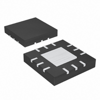
MAX1932ETC+T Maxim Integrated Products, MAX1932ETC+T Datasheet

MAX1932ETC+T
Specifications of MAX1932ETC+T
Related parts for MAX1932ETC+T
MAX1932ETC+T Summary of contents
Page 1
... MAX1932 ________________________________________________________________ Maxim Integrated Products For pricing, delivery, and ordering information, please contact Maxim/Dallas Direct! at 1-888-629-4642, or visit Maxim’s website at www.maxim-ic.com. Safest APD Bias Supply ♦ Small Circuit Footprint ♦ Circuit Height < 2mm ♦ 2.7V to 5.5V Input ♦ 4.5V to 90V Output ♦ ...
Page 2
Digitally Controlled, 0.5% Accurate, Safest APD Bias Supply ABSOLUTE MAXIMUM RATINGS VIN to GND...............................................................-0.3V to +6V DIN, SCLK, CS GND ......................................-0.3V to +6V COMP, DACOUT, GATE GND ...........-0. CS+, CS- to GND .................................................-0.3V to ...
Page 3
Digitally Controlled, 0.5% Accurate, ELECTRICAL CHARACTERISTICS (continued) = 3.3V SCLK = 3.3V, CS+ = CS- = 45V, Circuit of Figure PARAMETER SYMBOL DIGITAL INPUTS (DIN, SCLK, CS) Input Low Voltage Input ...
Page 4
Digitally Controlled, 0.5% Accurate, Safest APD Bias Supply ELECTRICAL CHARACTERISTICS (continued) = 3.3V SCLK = 3.3V, CS+ = CS- = 45V, Circuit of Figure PARAMETER SYMBOL FB Voltage FB to COMP ...
Page 5
Circuit of Figure SWITCHING WAVEFORMS MAX1932 toc01 RIPPLE (AC-COUPLED) OUT V = 90V OUT 1μs/div OUTPUT VOLTAGE vs. INPUT VOLTAGE 2.5 3.5 4.5 ...
Page 6
Digitally Controlled, 0.5% Accurate, Safest APD Bias Supply PIN NAME 1 SCLK DAC Serial Clock Input 2 DIN DAC Serial Data Input CL Current-Limit Indicator Flag indicates that the part is in current limit. Logic high level ...
Page 7
Digitally Controlled, 0.5% Accurate, Output and DAC Adjustments Range Many biasing applications require an adjustable output voltage, which is easily obtained using the MAX1932’s DAC output (Figure 2). The DAC output voltage is given by the following equation: ⎛ 1 ...
Page 8
Digitally Controlled, 0.5% Accurate, Safest APD Bias Supply (<10pF) are recommended to minimize losses. A small- signal silicon switching diode is suitable if efficiency is not critical. Output Filter Capacitor Selection The output capacitors of the MAX1932 must have high ...
Page 9
Digitally Controlled, 0.5% Accurate, Table 1. Compensation Components for Typical Circuits (Figure 2) INDUCTOR OUT OUT(MAX) (µ 40-90V at 2.5mA 100 IN OUT 5V , 20-60V at 2.5mA 150 IN OUT ...
Page 10
Digitally Controlled, 0.5% Accurate, Safest APD Bias Supply COMP REF 1.25V FB 987kΩ CS+ 987kΩ CS- SCLK 8 SPI SERIAL DIN INTERFACE CS Figure 1. Functional Diagram 10 ______________________________________________________________________________________ UVLO ERROR AMPLIFIER ERROR COMPARATOR RAMP OSC CLIM 13kΩ 13kΩ REF ...
Page 11
Digitally Controlled, 0.5% Accurate, 2.7V TO 5.5V R7 20kΩ C4 0.22μF Figure 2. Typical Operating Circuit GATE FB MAX1932 CS+ CS- Figure 3. Taking Feedback Ahead of Output Filter ______________________________________________________________________________________ Safest APD Bias Supply C1 1μF INPUT L1 VIN CL ...
Page 12
Digitally Controlled, 0.5% Accurate, Safest APD Bias Supply CS t CSH0 t CSS0 SCLK t DS DIN Figure 5. Detailed Serial Interface Timing Diagram 12 ______________________________________________________________________________________ CSW t CSH1 t CSS1 ...
Page 13
Digitally Controlled, 0.5% Accurate, 120 100 0.01 Figure 6. Loop Response ______________________________________________________________________________________ Safest APD Bias Supply 90V, 1mA POLE1 0.0023Hz ZERO1 36Hz POLE2 36Hz POLE3 4.2kHz A 102dB OL 0.1 1.0 10 FREQUENCY (Hz) 90V, 2.5mA ...
Page 14
Digitally Controlled, 0.5% Accurate, Safest APD Bias Supply MAX1932 Figure 7. Adding a Post LC Filter Figure 8. Adding an NTC Thermistor for Hardware Temperature Compensation; Output Voltage Increases with Temperature Rise 14 ______________________________________________________________________________________ VIN GATE FB CS+ CS- VIN ...
Page 15
Digitally Controlled, 0.5% Accurate, (The package drawing(s) in this data sheet may not reflect the most current specifications. For the latest package outline information www.maxim-ic.com/packages.) ______________________________________________________________________________________ Safest APD Bias Supply Package Information PACKAGE OUTLINE, 12, 16, 20, 24, ...
Page 16
... Maxim cannot assume responsibility for use of any circuitry other than circuitry entirely embodied in a Maxim product. No circuit patent licenses are implied. Maxim reserves the right to change the circuitry and specifications without notice at any time. 16 ____________________Maxim Integrated Products, 120 San Gabriel Drive, Sunnyvale, CA 94086 408-737-7600 © 2002 Maxim Integrated Products ...


